Reliability evaluating method of electronic packaging micro-welding spot

A technology for electronic packaging and evaluation methods, applied in welding equipment, metal processing equipment, material thermal development and other directions, can solve problems such as limited temperature gradient range, inability to effectively evaluate the reliability of electronic packaging micro-solder joints, and achieve consistent thickness and preparation. Stable and reliable, good contact effect

Inactive Publication Date: 2019-05-28
CHONGQING UNIV OF TECH
View PDF8 Cites 6 Cited by
  • Summary
  • Abstract
  • Description
  • Claims
  • Application Information

AI Technical Summary

Problems solved by technology

However, it only has a heating device at one end of the solder joint, and the other end is kept at room temperature. The range of temperature gradients that can be loaded is limited, and it cannot effectively evaluate the reliability of micro-solder joints in electronic packaging under extreme temperature gradient ranges.

Method used


Image

  • Reliability evaluating method of electronic packaging micro-welding spot
  • Reliability evaluating method of electronic packaging micro-welding spot
  • Reliability evaluating method of electronic packaging micro-welding spot

Examples


Embodiment 1

[0029] Embodiment 1, a method for evaluating the reliability of micro-solder joints in electronic packaging, which includes the following steps.

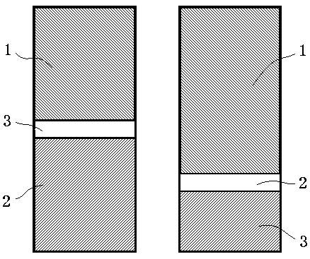
[0030] 1) Select the first metal plate and the second metal plate whose material is pure Co, see figure 2 , the thickness of the first metal plate 1 is 7.2 mm, and the thickness of the second metal plate 2 is 3.6 mm. It should be noted here that the thickness of the first metal plate 1 and the second metal plate 2 can also be the same, and the second The thickness of the second metal plate 2 is set to be smaller than the first metal plate 1, so that the micro-soldering point is as close as possible to the hot end, has higher capacity, and is more prone to thermal migration; then the first metal plate 1 and the second metal plate 2 Apply flux to the opposite welding surface, align the welding surfaces of the first metal plate 1 and the second metal plate 2, and use a mica sheet with a thickness of 70 μm to separate the first metal p...

Embodiment 2

[0035] Embodiment 2, a method for evaluating the reliability of micro-solder joints in electronic packaging, which includes the following steps.

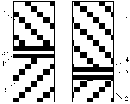
[0036] 1) Select the first metal plate and the second metal plate made of pure Cu, the thickness of the first metal plate is 7.2mm, and the thickness of the second metal plate is 3.6mm, and then use electroplating, electrodeposition or sputtering on the Prepare the first metal layer and the second metal layer whose material is Co-3.5at%P on the first metal plate and the second metal plate, and then coat flux on the opposite welding surface of the first metal layer and the second metal plate Align the welding surfaces of the first metal layer and the second metal layer, separate the first metal layer and the second metal layer with a mica sheet with a thickness of 70 μm, and perform dip soldering at a temperature of 320 ° C. The material is pure Sn, an intermetallic compound is formed at the contact point between the first metal laye...


PUM

PropertyMeasurementUnit
Weld widthaaaaaaaaaa
Heightaaaaaaaaaa
Thicknessaaaaaaaaaa

Abstract

The invention discloses a reliability evaluating method of an electronic packaging micro-welding spot. The method includes the following steps of firstly, selecting a first metal plate and a second metal plate for surface treatment, and welding the welding surfaces of the first metal plate and the second metal plate through brazing; secondly, cutting the welded first metal plate and second metal plate to prepare a sample; thirdly, vertically placing the sample in a temperature loading device, forming the temperature gradient at the upper end and the lower end of the micro-welding spot of the sample, and starting to record the loading time when the temperature is stabilized; fourthly, loading different times to the sample under the temperature gradient in the third step, and evaluating thereliability of the electronic packaging micro-welding spot within the region of the temperature gradient by analyzing the thickness variation conditions of intermetallic compounds under the differentloading times. The stable and controllable temperature gradient can be obtained, the temperature gradient range is large, and therefore the reliability of the electronic packaging micro-welding spot in the region of the extreme temperature gradient can be effectively evaluated.

Description

technical field [0001] The invention relates to the reliability of electronic packaging, in particular to a method for evaluating the reliability of electronic packaging micro solder joints. Background technique [0002] In the environment of the Internet of Things and artificial intelligence, the extreme pursuit of high-density system integration and excellent performance of electronic terminal products has prompted the rapid development of various chip stacking solutions such as three-dimensional packaging technology. High-end electronic system products, such as service workstations, portable multimedia devices, digital imaging devices, etc., all emphasize computing speed and stability. In addition, semiconductor technology has entered the nanometer scale, and more transistors can be manufactured on IC chips. At the same time, IC packaging technology is also developing towards precision and miniaturization. In its development trend, one of the biggest obstacles comes from...

Claims


Application Information

Patent Timeline
IPC IPC(8): G01N25/20B23K1/00
Inventor 杨栋华杜飞张春红甘贵生冉藤翟翔陈新年施雷
Owner CHONGQING UNIV OF TECH
Why Eureka
Try Eureka