OLED display panel and preparation method thereof

A display panel and display area technology, applied in semiconductor/solid-state device manufacturing, electrical components, electric solid-state devices, etc., can solve problems such as device damage, and achieve the effect of promoting adhesion strength

Active Publication Date: 2019-05-28
WUHAN CHINA STAR OPTOELECTRONICS SEMICON DISPLAY TECH CO LTD
View PDF9 Cites 7 Cited by
  • Summary
  • Abstract
  • Description
  • Claims
  • Application Information

AI Technical Summary

Problems solved by technology

[0005] The invention provides an OLED display panel to solve the technical problem that wat

Method used


Image

  • OLED display panel and preparation method thereof
  • OLED display panel and preparation method thereof
  • OLED display panel and preparation method thereof

Examples


Embodiment 1

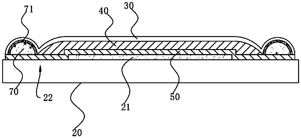
[0043] A kind of OLED display panel, such as figure 2 As shown, the OLED display panel includes a display device board 20 and a dam 70 made of silicone resin; the display device board 20 includes a display area 21 and a non-display area 22, and the dam 70 surrounds the display A region 21 is provided and located at the non-display region 22 .

[0044] Wherein, the OLED display panel further includes an organic buffer layer 40 covering the display area 21, and a first inorganic layer 30 covering the organic buffer layer 40 and the bank 70; the organic buffer layer 40 is located The inner side of the bank dam 70 , and the edge of the organic buffer layer 40 is in contact with the inner side of the bank dam 70 .

[0045] Wherein, the cofferdam 70 includes a weir body, and the surface of the weir body is treated with plasma to form a hardened layer 71 .

[0046] The cofferdam 70 is used to prevent water and oxygen from invading from the side of the OLED display panel, and the s...

Embodiment 2

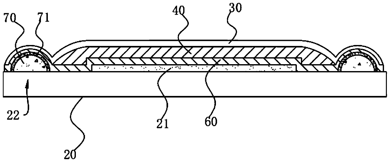
[0059] A kind of OLED display panel, such as image 3 As shown, the difference from Embodiment 1 is that no second inorganic layer 50 is provided, and a third inorganic layer 60 covering the display area 21 and the bank dam 70 is provided on the display device panel 20 , the organic buffer layer 40 is disposed on the third inorganic layer 60 .

[0060] Further, the edge of the first inorganic layer 30 and the edge of the third inorganic layer 60 are located outside the bank 70, and the edge of the first inorganic layer 30 and the third inorganic layer 60 The distance between the edges of each and the outer side of the cofferdam 70 in the horizontal direction is 1-3 microns.

[0061] In one embodiment, the distance between the edge of the first inorganic layer 30 and the edge of the third inorganic layer 60 and the outside of the bank 70 in the horizontal direction is 1 μm.

Embodiment 3

[0063] Based on the OLED display panel in Example 1, a method for preparing an OLED display panel is proposed, such as Figure 4 shown, including the following steps:

[0064] S10, providing a display device board 20;

[0065] S20, forming a bank dam 70 surrounding the display area 21 at the non-display area 22 of the display device panel 20;

[0066] S30, using plasma to perform surface treatment on the surface of the cofferdam 70 to form a hardened layer 71;

[0067] S40, forming an organic buffer layer 40 covering the display area 21 inside the bank 70;

[0068] S50 , forming the first inorganic layer 30 covering the organic buffer layer 40 and the banks 70 on the organic buffer layer 40 .

[0069] Further, before the step S20, the method for preparing the OLED display panel further includes:

[0070] S60 , forming a second inorganic layer 50 covering the display area 21 and extending to the non-display area 22 on the display device panel 20 .

[0071] Such as Figure...


PUM

PropertyMeasurementUnit
Thicknessaaaaaaaaaa
Thicknessaaaaaaaaaa
Thicknessaaaaaaaaaa

Abstract

The invention provides an OLED display panel. The OLED display panel comprises a display device plate and a cofferdam; the cofferdam is arranged around a display area on the display device plate and is located at a non-display area; the OLED display panel further comprises an organic buffer layer covering the display area and a first inorganic layer covering the organic buffer layer and the cofferdam; the organic buffer layer is located on the inner side of the cofferdam, and the edge of the organic buffer layer is in contact with the inner side of the cofferdam. Beneficial effects are as follows: the surface of the cofferdam is treated by using plasma; under the oxidation action of the plasma, a hardened layer between organic silicon and inorganic silicon is formed on the surface of the weir body; active resistance to water and oxygen invasion of the side surface of the OLED display panel is facilitated, meanwhile, the plasma treated hardened layer can effectively promote the adhesionstrength of the inorganic layer and the cofferdam, and the risk of debonding and cracking at the edge of the first inorganic layer and the edge of the organic buffer layer in the bending process of the OLED display panel is reduced.

Description

technical field [0001] The invention relates to the field of display technology, in particular to an OLED display panel and a preparation method thereof. Background technique [0002] In recent years, OLED, as the most promising technology in the field of flexible display, has attracted a lot of attention. The lifetime of an OLED device depends on the material selected for the light-emitting device on the one hand, and on the other hand the packaging method of the device. So far, it has become a mainstream packaging method in the industry to use a thin-film encapsulation (TFE) structure in which organic and inorganic films are stacked to package and protect OLED devices. [0003] Such as figure 1 In the thin film packaging structure shown, the dense inorganic film layer 11 plays the role of blocking water and oxygen, and the thicker and soft organic film layer 12 plays the role of planarization and slow release of stress. The two together constitute the TFE layer . [00...

Claims


Application Information

Patent Timeline
IPC IPC(8): H01L27/32H01L51/52H01L51/56
Inventor 张文智
Owner WUHAN CHINA STAR OPTOELECTRONICS SEMICON DISPLAY TECH CO LTD
Why Eureka
Try Eureka