A self-adaptive bias radio frequency power amplifier

A technology of adaptive bias and RF power, which is applied in power amplifiers, high-frequency amplifiers, amplifier input/output impedance improvements, etc., can solve the problem of no improvement in gain compression, delay gain compression, and improve AM-PM offset , Improve the effect of AM-AM imbalance

Pending Publication Date: 2019-05-28
RDA MICROELECTRONICS TECH SHANGHAI CO LTD
View PDF10 Cites 9 Cited by
  • Summary
  • Abstract
  • Description
  • Claims
  • Application Information

AI Technical Summary

Problems solved by technology

The disadvantage of this solution is that the technical means to improve the linearity does not directly act on the amplifying transistor, but directly acts on the withstand voltage transistor. It is to improve the AM-AM offset and AM-PM offset through an indirect way, and there is still an improvement. space
This scheme also does not improve gain compression, and there is room for improvement in AM-AM offset

Method used


Image

  • A self-adaptive bias radio frequency power amplifier
  • A self-adaptive bias radio frequency power amplifier
  • A self-adaptive bias radio frequency power amplifier

Examples


Embodiment 1

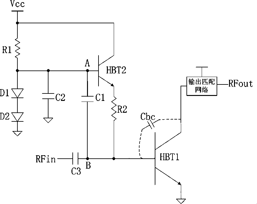
[0034] see figure 2 , which is Embodiment 1 of an adaptively biased radio frequency power amplifier provided by the present application, mainly including an amplifying circuit and a biasing circuit.

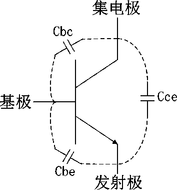
[0035] The amplifying circuit mainly includes a power transistor HBT1, such as gallium arsenide HBT. The radio frequency input signal RFin is connected to the base of the power transistor HBT1 through the capacitor C3, the emitter of the power transistor HBT1 is grounded, and the collector outputs an amplified radio frequency signal. The amplified radio frequency signal is subjected to impedance matching through an output matching network to obtain a radio frequency output signal RFout. There is a base-collector parasitic capacitance Cbc between the base and the collector of the power transistor HBT1, which is one of the main factors causing the nonlinearity of the power transistor HBT1.

[0036] The bias circuit mainly includes a bias transistor HBT2, such as GaAs HBT. A res...

Embodiment 2

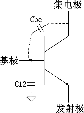
[0048] In the bias circuit of the second embodiment, the bias transistor HBT2 and the mirror transistor HBT3 constitute a current mirror. The working principle of the second embodiment is similar to that of the first embodiment. On the one hand, the base-collector parasitic capacitance Cbc of the power transistor HBT1 is grounded through the capacitance series branch composed of the first capacitor C1 and the second capacitor C2 in the bias circuit, which improves the AM-PM offset of the RF power amplifier and improves the linearity. On the other hand, capacitor one C1 couples the radio frequency input signal RFin to the base of the bias transistor HBT2, and capacitor two C2 reduces the impedance of the bias circuit so that the radio frequency input signal RFin is more easily coupled to the bias transistor HBT2, which improves the radio frequency The AM-AM offset of the power amplifier also improves the linearity. Embodiment 2 also directly improves the AM-PM offset and AM-A...


PUM


Abstract

The invention discloses a self-adaptive bias radio frequency power amplifier which comprises an amplifying circuit and a bias circuit. Wherein the amplifying circuit is provided with a power transistor, the biasing circuit is provided with a biasing transistor, and an emitting electrode of the biasing transistor is connected with a base electrode of the power transistor through a resistor to provide biasing current and / or biasing voltage for the base electrode. A capacitor series branch is also arranged in the biasing circuit and is formed by connecting at least two capacitors in series. One end of the capacitor series branch is connected with the base of the power transistor, and the other end is grounded. Base-to-base of power transistor is reduced. The adverse effect of the parasitic capacitance of the collector on the linearity is improved, and the AM-of the radio frequency power amplifier is improved. PM imbalance; The gain compression phenomenon of the radio frequency power amplifier is delayed, and the AM-AM imbalance of the radio frequency power amplifier is improved.

Description

technical field [0001] This application relates to a radio frequency power amplifier. Background technique [0002] With the development of mobile communication technology, data traffic is constantly increasing, and spectrum resources are becoming increasingly exhausted. In order to solve such problems, modern mobile communication systems generally use linear modulation techniques, such as QPSK (Quadrature Phase Shift Keying, quadrature phase shift keying), QAM (Quadrature Amplitude Modulation, quadrature amplitude modulation), HPSK (Hybrid Phase Shift Keying, hybrid Phase Shift Keying), OFDM (Orthogonal Frequency Division Multiplexing, Orthogonal Frequency Division Multiplexing), etc. The signals generated by the above modulation methods are all modulated signals with non-constant envelopes, and the system is multi-carrier and multi-channel, and the peak-to-average ratio (PAR, Peak-to-Average Ratio) of the signal is very large. [0003] The radio frequency power amplifier...

Claims


Application Information

Patent Timeline
Patent Type & Authority Applications(China)
IPC IPC(8): H03F3/19H03F3/24H03G3/30H03F1/56
Inventor 章乐李啸麟陈文斌徐李娅贾斌
Owner RDA MICROELECTRONICS TECH SHANGHAI CO LTD
Why Eureka
Try Eureka