Preprocessing method and wafer processing method

A pretreatment, wafer technology, applied to circuits, discharge tubes, electrical components, etc., can solve problems such as residues on the chamber wall that cannot be removed, wear of components in the chamber, offset etching rate, etc., to reduce regular maintenance. time, improve component utilization, and improve the effect of thickness uniformity

Active Publication Date: 2021-06-08
BEIJING NAURA MICROELECTRONICS EQUIP CO LTD
View PDF4 Cites 0 Cited by
  • Summary
  • Abstract
  • Description
  • Claims
  • Application Information

AI Technical Summary

Problems solved by technology

[0003] However, during the process of the etching chamber, the deviation of process results (including etching rate deviation and critical dimension deviation) caused by process residues, hardware loss and aging, and the accumulation of particles The increase in the number of defects is an unavoidable problem in the mass production process. Therefore, how to maintain the stability of the chamber and the consistency of the initial process environment between different wafers, as well as reduce the number of particles in the chamber, is a key step in the process node. An important issue in the development process
[0004] At present, the commonly used solution is to use inter-chip dry cleaning and regular maintenance to ensure that the chamber environment between different wafers is as consistent as possible during the mass production process. However, the internal environment of the chamber will continue to change during long-term use. , resulting in residues on the chamber wall that cannot be removed, and a certain degree of wear and tear on the inner parts of the chamber under the long-term bombardment of the plasma

Method used


Image

  • Preprocessing method and wafer processing method
  • Preprocessing method and wafer processing method
  • Preprocessing method and wafer processing method

Examples


Embodiment Construction

[0037] In order to enable those skilled in the art to better understand the technical solution of the present invention, the preprocessing method and wafer processing method provided by the present invention will be described in detail below in conjunction with the accompanying drawings.

[0038] Please also refer to Figure 1 to Figure 2C , the pretreatment method provided by the invention, it comprises:

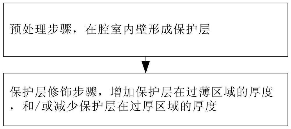
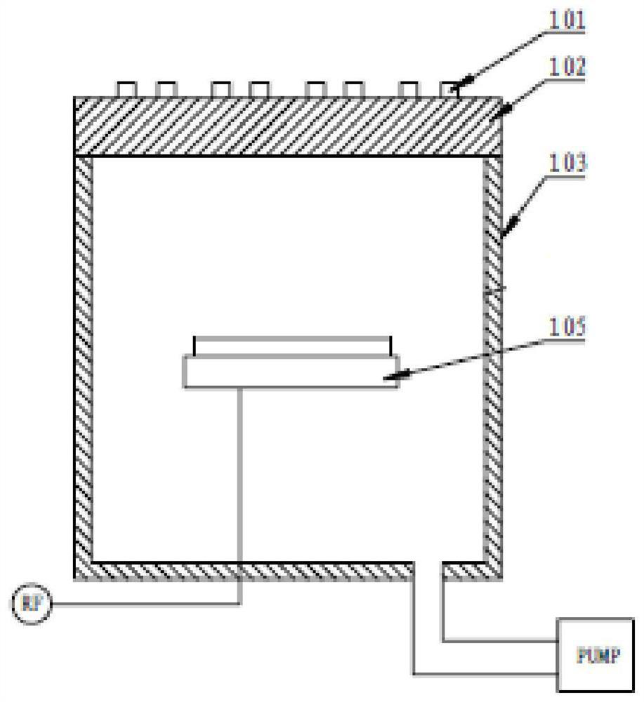
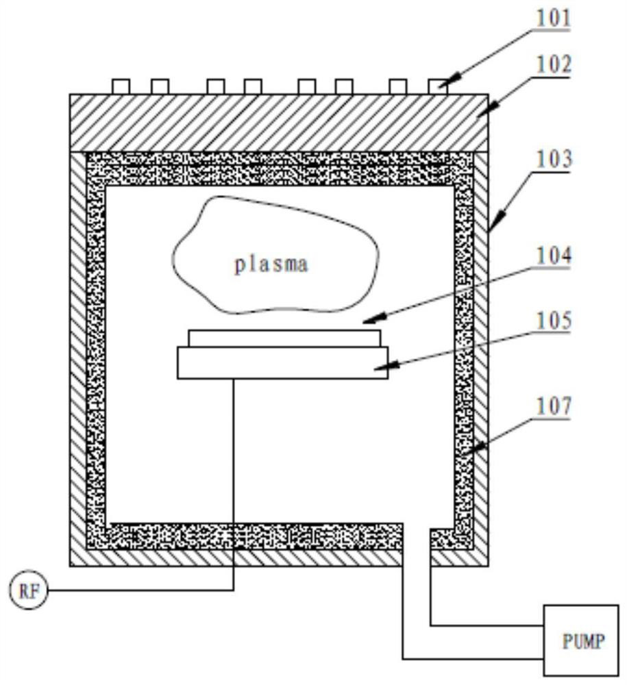
[0039] A pretreatment step, forming a protective layer 107 on the inner wall 103 of the chamber;

[0040] The protective layer modifying step is to increase the thickness of the protective layer 107 in the over-thin area, and / or decrease the thickness of the protective layer 107 in the over-thick area.

[0041] With the help of the protective layer 107, the metal and particles on the chamber inner wall 103 can be prevented from falling on the wafer surface during the process, thereby improving the product yield.

[0042] By means of the above-mentioned protective layer mo...


PUM


Abstract

The present invention provides a pretreatment method and a wafer treatment method. The pretreatment method comprises: a pretreatment step of forming a protective layer on the inner wall of a chamber; a protective layer modification step of increasing the thickness of the protective layer in an over-thin area, and / or reducing The thickness of the protective layer in the overthick area. The pretreatment method provided by the present invention can not only prevent the metal and particles on the chamber wall from falling on the wafer surface during the process by forming a protective layer, but also improve the uniformity of the protective layer, thereby improving the process Defects and reduce component loss due to missing protective layers.

Description

technical field [0001] The invention relates to the technical field of semiconductor manufacturing, in particular to a preprocessing method and a wafer processing method. Background technique [0002] In the semiconductor manufacturing industry, with the continuous update of the integrated circuit process and the continuous progress of the process node, the requirements for the uniformity and stability of the etching process and the etching chamber, as well as the consistency of the key dimensions of the process results, are becoming more and more demanding. come higher. [0003] However, during the process of the etching chamber, the deviation of process results (including etching rate deviation and critical dimension deviation) caused by process residues, hardware loss and aging, and the accumulation of particles The increase in the number of defects is an unavoidable problem in the mass production process. Therefore, how to maintain the stability of the chamber and the c...

Claims


Application Information

Patent Timeline
Patent Type & Authority Patents(China)
IPC IPC(8): H01J37/32
Inventor 张宇
Owner BEIJING NAURA MICROELECTRONICS EQUIP CO LTD
Why Eureka
Try Eureka