Method for sorting silicon wafers according to their bulk lifetime

A bulk lifetime, wafer technology, applied in crystal growth, chemical instruments and methods, sorting, etc., can solve problems such as inability to optimally optimize homojunction cells

Active Publication Date: 2019-06-04
COMMISSARIAT A LENERGIE ATOMIQUE ET AUX ENERGIES ALTERNATIVES
View PDF14 Cites 2 Cited by
  • Summary
  • Abstract
  • Description
  • Claims
  • Application Information

AI Technical Summary

Problems solved by technology

[0010] Additionally, this method of sorting wafers does not allow for optimal optimization of the fabrication of homojunction cells, as it requires that the first step of the fabrication method be completed in each case One step: Diffusion of the emitter (e.g. 10 seconds at 800°C)
This step represents unnecessary overhead when wafers are eventually discarded

Method used


Image

  • Method for sorting silicon wafers according to their bulk lifetime
  • Method for sorting silicon wafers according to their bulk lifetime
  • Method for sorting silicon wafers according to their bulk lifetime

Examples


Embodiment Construction

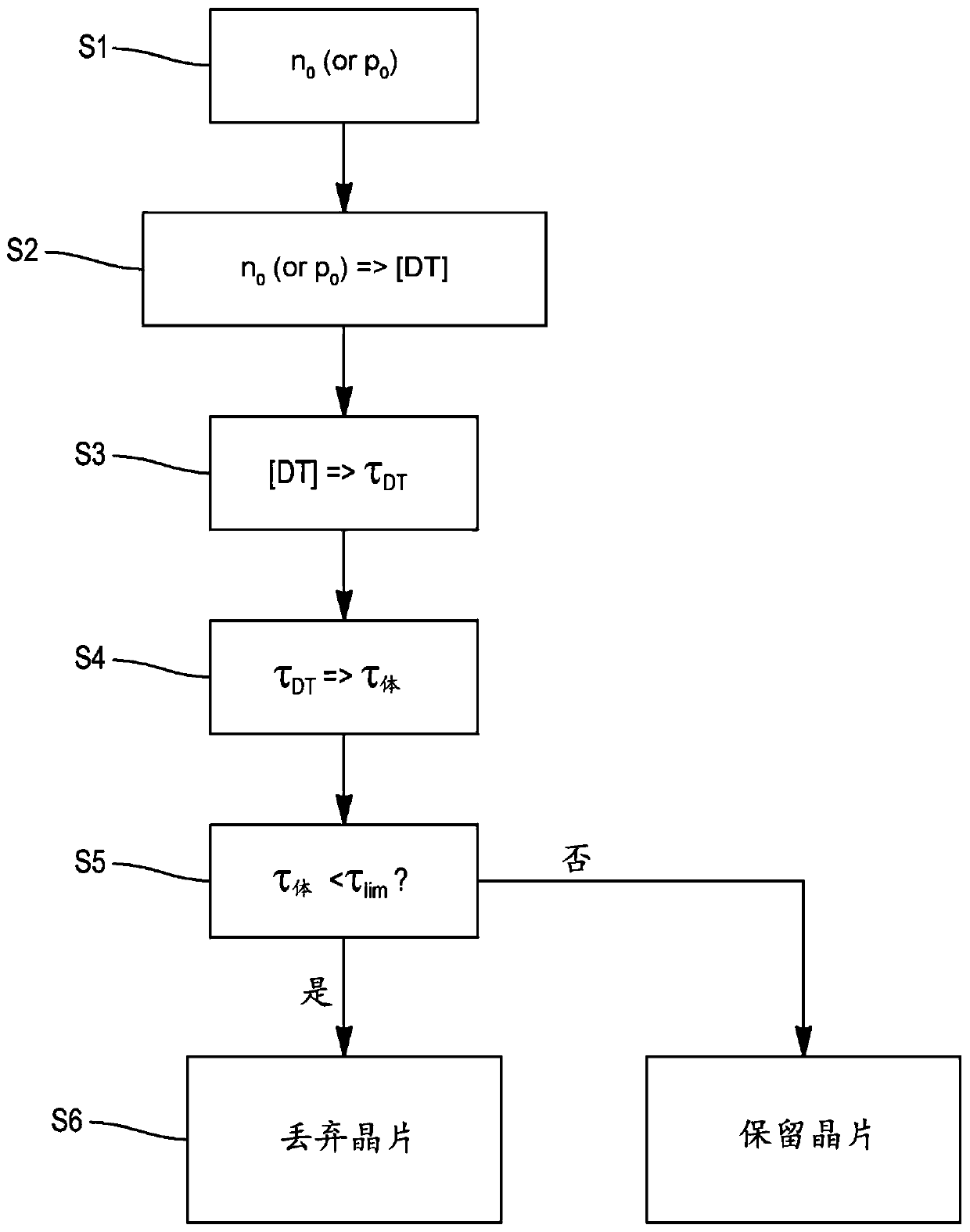
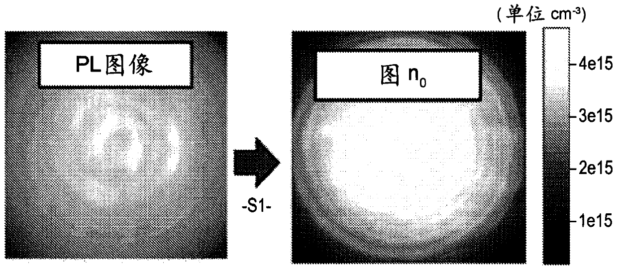
[0060] Single crystal silicon ingots obtained by the Czochralski (CZ) method contain a large number of thermal donors because the silicon has a high concentration of interstitial oxygen and cools slowly. These thermal donors are then found in silicon wafers originating from cut ingots.

[0061] Thermal donors have two effects on the properties of silicon. First, they affect the majority free charge carrier concentration, often referred to as net doping, since each thermal donor generates two free electrons. Second, certain thermal donors act as recombination centers for electron-hole pairs, which limits the bulk lifetime of charge carriers.

[0062] The sorting method described below exploits these two effects to determine the thermal donor concentration from the majority free charge carrier concentration, and to determine the thermal donor-limited lifetime from the thermal donor concentration, respectively.

[0063] These methods are performed while the wafer is preferably ...


PUM


Abstract

The invention relates to a Czochralski-type method for sorting wafers obtained by cutting a single-crystal silicon ingot, the method being implemented when the wafers are in an as-cut state or in a shaped-surface state. The method comprises the following steps: a) measuring the majority free charge carrier concentration in at least one area of each wafer; b) calculating the thermal donor concentration in said area of each wafer, on the basis of the majority free charge carrier concentration; c) calculating the charge carrier lifetime limited by the thermal donors in said area of each wafer, onthe basis of the thermal donor concentration; d) determining a bulk lifetime value for the charge carriers in each wafer on the basis of the lifetime limited by the thermal donors; e) comparing the bulk lifetime value or a normalised bulk lifetime value with a threshold value; and f) discarding the wafer when the bulk lifetime value or the normalised bulk lifetime value is lower than the threshold value.

Description

technical field [0001] The present invention relates to a method for sorting silicon wafers before they are cut from an ingot and before they are used in the manufacture of semiconductor devices such as solar cells. Background technique [0002] About 10% to 20% of monocrystalline silicon wafers obtained by the Czochralski method are incompatible with the manufacture of high-efficiency solar cells. Indeed, these wafers contain defects that limit the lifetime of the photogenerated charge carriers and lead to a reduction in efficiency, which can be as high as 4% (absolute). [0003] Life-limiting defects include thermal donors (DT). Thermal donors are aggregates generated by interstitial oxygen contained in silicon (ie, oxygen atoms occupy interstitial positions in the crystal lattice). They are formed during ingot drawing when the temperature of the silicon is between 350°C and 500°C. [0004] The wafer which has the highest donor concentration and thus can limit its effic...

Claims


Application Information

Patent Timeline
Patent Type & Authority Applications(China)
IPC IPC(8): H01L31/18C30B29/06
CPCH01L31/1804Y02E10/547Y02P70/50H01L22/20H01L22/12H01L21/67271C30B29/06H01L21/78B07C5/344
Inventor 埃莉诺·莱蒂维尔弗里德·法夫尔乔迪·韦尔曼
Owner COMMISSARIAT A LENERGIE ATOMIQUE ET AUX ENERGIES ALTERNATIVES
Why Eureka
Try Eureka