Structure and manufacturing method of a medium and high voltage trench type power metal oxide half field effect transistor

A metal oxide half-field and manufacturing method technology, applied in semiconductor/solid-state device manufacturing, transistors, semiconductor devices, etc., can solve problems such as device performance degradation, and achieve the effect of improving the application range

Active Publication Date: 2022-02-15
江苏应能微电子股份有限公司
View PDF4 Cites 0 Cited by
  • Summary
  • Abstract
  • Description
  • Claims
  • Application Information

AI Technical Summary

Problems solved by technology

[0004] The technical problem to be solved by the present invention is: when a voltage collapse occurs in a medium-high voltage MOSFET device, a large electric field will be accumulated at the node as its collapse point, and the current will stay in the drain metal layer or the gate oxide layer and lead to it. The phenomenon of device performance degradation, the present invention provides a structure and manufacturing method of a medium and high voltage trench power metal oxide half field effect transistor to solve the above problems

Method used


Image

  • Structure and manufacturing method of a medium and high voltage trench type power metal oxide half field effect transistor
  • Structure and manufacturing method of a medium and high voltage trench type power metal oxide half field effect transistor
  • Structure and manufacturing method of a medium and high voltage trench type power metal oxide half field effect transistor

Examples


Embodiment Construction

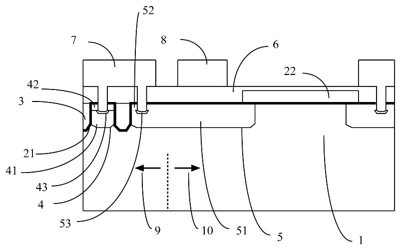
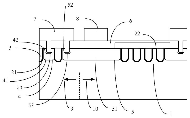
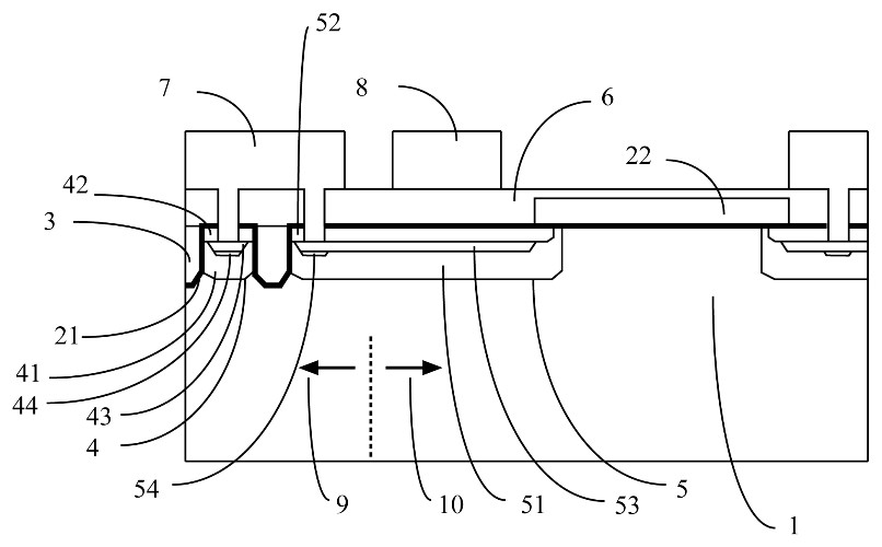
[0054] Embodiments of the present invention are described in detail below, and examples of the embodiments are shown in the drawings, wherein the same or similar reference numerals denote the same or similar components or components having the same or similar functions throughout. The embodiments described below by referring to the figures are exemplary only for explaining the present invention and should not be construed as limiting the present invention.

[0055] In the description of the present invention, it should be understood that the orientation or positional relationship indicated by the terms "upper", "lower surface", "side", "side", "horizontal plane" etc. is based on the orientation or position shown in the drawings The relationship is only for the convenience of describing the present invention and simplifying the description, but does not indicate or imply that the referred device must have a specific orientation, be constructed and operated in a specific orientat...


PUM

PropertyMeasurementUnit
thicknessaaaaaaaaaa
thicknessaaaaaaaaaa
thicknessaaaaaaaaaa

Abstract

The invention provides a structure and a manufacturing method of a medium and high voltage trench type power metal oxide half field effect transistor, comprising: a substrate+epitaxy, an oxide layer, a gate oxide layer, and a polysilicon (Poly-Si ) layer, a field oxide layer, a first doped region, a second doped region, a first implanted first P+ doped region, a first implanted second P+ doped region, a dielectric Layer (ILD), a second implantation of the first P+ doped region, a second implantation of the second P+ doped region, a first metal layer, a second metal layer, the present invention uses deep ion implantation techniques, Change the current path from the original P-doped region to the P+ doped region when the voltage collapses. Since the resistance of the P+ doped region is small, the product of the current and the path resistance is not likely to be greater than the Vbe of the built-in parasitic dual-stage transistor The voltage allows the triode to be turned on, so it is easy to maintain the original avalanche breakdown (UIS) capability and reduce the probability of snapback. The invention can complete medium and high voltage products, greatly improving the application range of the product.

Description

technical field [0001] The invention relates to electronic components, semiconductors and integrated circuits, and in particular to a structure and a manufacturing method of a medium-high voltage trench type power metal oxide half-field-effect transistor. Background technique [0002] The structure of Power MOSFET (Metal-Oxide-SemiconductorField-Effect-Transistor) can be divided into trench structure and planar structure. The trench structure is due to the cell size (Cell Pitch ) is small, and better resistance can be obtained, so it is widely used in voltages below 200V, and above 200V, because the relationship between resistance and cell size is low, it is mostly completed with a planar structure. [0003] The current simple trench (trench) structure of MOSFET is as follows: figure 1 As shown, the cross-sectional structure can be divided into the active area and the terminal area, and the number of masks generated by it is five if the passivation layer (passivation) is no...

Claims


Application Information

Patent Timeline
Patent Type & Authority Patents(China)
IPC IPC(8): H01L29/786H01L21/266H01L29/06H01L21/336
Inventor 李振道孙明光
Owner 江苏应能微电子股份有限公司
Why Eureka
Try Eureka