Organic light-emitting diode and preparation method thereof
A luminescent and diode technology, applied in the field of organic electroluminescent diodes and its preparation, can solve the problems of OLED life reduction, light-emitting device life short, energy loss, etc., to reduce efficiency roll-off, improve device life, and prolong service life Effect
- Summary
- Abstract
- Description
- Claims
- Application Information
AI Technical Summary
Problems solved by technology
Method used
Image

Examples
Embodiment 1
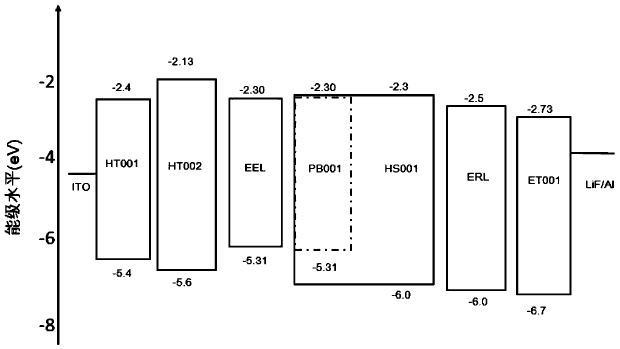
[0046] The energy level distribution situation of each material in embodiment 1 is as image 3 shown.
[0047] In order to reflect the technical effect of the device of Example 1, the comparative device of Example 1 (device 1-2) without an efficiency enhancing layer and without an exciton delay layer is used as a comparison:
[0048] ITO / HT001(60nm) / HT002(5nm) / EHS001:PB001(50nm, 8wt%) / ET001(25nm) / LIF(1nm) / Al(100nm).
[0049] The performance data are shown in Table 1 below:
[0050] Table 1 Embodiment 1 device performance comparison data
[0051]
[0052] Figure 4 It is a graph comparing the current density-voltage curves of device 1-1 and device 1-2; from Figure 4 It can be seen that at the same voltage, the current density of device 1-1 is lower than that of device 1-2, because the mobility of the exciton delay layer is lower than that of the electron transport layer.
[0053] Figure 5 It is a graph comparing the brightness-voltage curves of device 1-1 and device ...
Embodiment 2
[0063] In order to reflect the technical effect of the device of Example 2, the comparative device of Example 2 (device 2-2) without the efficiency enhancement layer and the exciton delay layer is used as a comparison:
[0064] The performance data comparison of ITO / HT001(60nm) / HT002(5nm) / EHS001:PB001(50nm, 8wt%) / ET001(25nm) / LIF(1nm) / Al(100nm) is shown in Table 2 below:
[0065] Table 2 Embodiment 2 device performance comparison data
[0066]
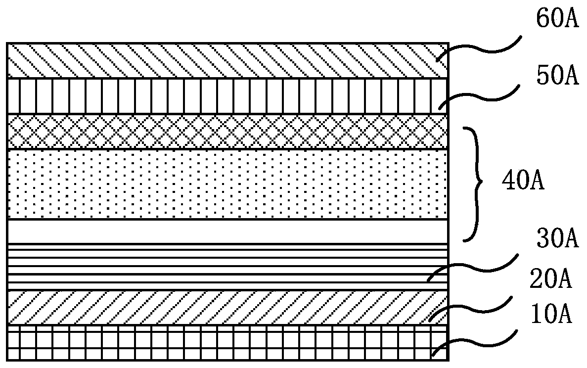
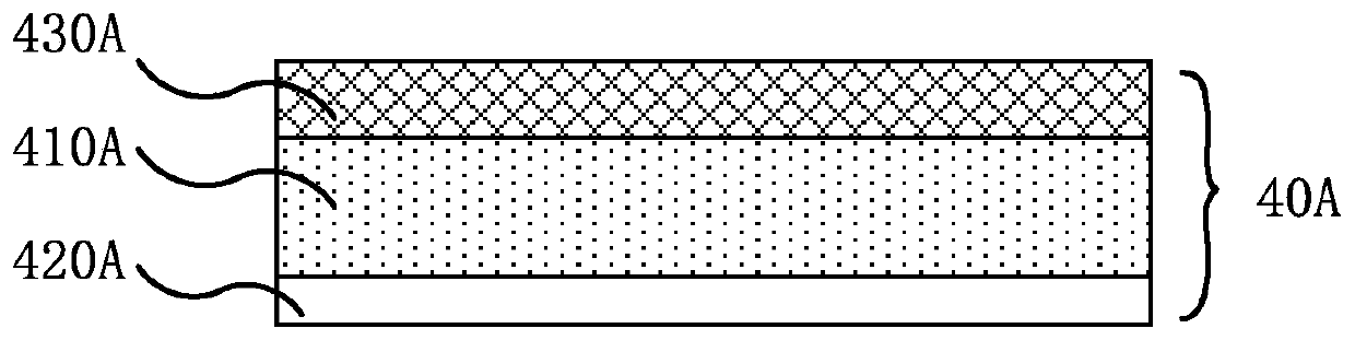
[0067] The third embodiment of the present invention relates to an organic electroluminescent diode, which is a modification of the organic electroluminescent diode of the first embodiment, and its structure is as follows: Figure 11 shown. The organic electroluminescent diode includes a substrate 10B, a first electrode 20B, a hole transport layer 30B, a composite light emitting unit 40B, an electron transport layer 50B and a second electrode 60B stacked in sequence. The composite light-emitting unit 40B in this embodiment includes...
Embodiment 3
[0074] In order to reflect the technical effect of the device of Example 3, the comparative device of Example 3 (device 3-2) without the efficiency enhancement layer and the exciton delay layer is used as a comparison:
[0075] ITO / HT001(65nm) / HHS001:PB001(50nm,8wt%) / ET001(25nm) / LIF(1nm) / Al(100nm)
[0076] The performance data comparison is shown in Table 3 below:
[0077] Table 3 Embodiment 3 device performance comparison data
[0078]
[0079] The fourth embodiment of the present invention relates to an organic electroluminescent diode, which is an improvement on the organic electroluminescent diode of the third embodiment, and its structure is as follows: Figure 13 shown. Specifically, in the composite light-emitting unit of the organic electroluminescent diode in this embodiment, the light-emitting unit group includes not only one light-emitting unit, but 2 to 64 light-emitting units stacked in sequence; wherein, the composition of each light-emitting unit It is the...
PUM
 Abstract
Description
Claims
Application Information
 - R&D
- Intellectual Property
- Life Sciences
- Materials
- Tech Scout
- Unparalleled Data Quality
- Higher Quality Content
- 60% Fewer Hallucinations
Browse by: Latest US Patents, China's latest patents, Technical Efficacy Thesaurus, Application Domain, Technology Topic, Popular Technical Reports.
© 2025 PatSnap. All rights reserved.Legal|Privacy policy|Modern Slavery Act Transparency Statement|Sitemap|About US| Contact US: help@patsnap.com