Eureka AIR delivers breakthrough ideas for toughest innovation challenges, trusted by R&D personnel around the world.

Light-emitting diode epitaxial wafer and growing method thereof

A technology of light-emitting diodes and growth methods, applied in the field of light-emitting diode epitaxial wafers and their growth, can solve problems such as the inability to effectively improve LED luminous efficiency, achieve the effects of reducing stress, reducing impact, and improving luminous efficiency

Active Publication Date: 2019-06-11
HC SEMITEK ZHEJIANG CO LTD
View PDF5 Cites 0 Cited by
  • Summary
  • Abstract
  • Description
  • Claims
  • Application Information

AI Technical Summary

Problems solved by technology

[0007] The embodiment of the present invention provides a light-emitting diode epitaxial wafer and a growth method thereof, which can solve the problem that the stress release layer in the prior art cannot effectively improve the luminous efficiency of the LED.

Method used


Image

  • Light-emitting diode epitaxial wafer and growing method thereof
  • Light-emitting diode epitaxial wafer and growing method thereof
  • Light-emitting diode epitaxial wafer and growing method thereof

Examples


Embodiment Construction

[0027] In order to make the object, technical solution and advantages of the present invention clearer, the implementation manner of the present invention will be further described in detail below in conjunction with the accompanying drawings.

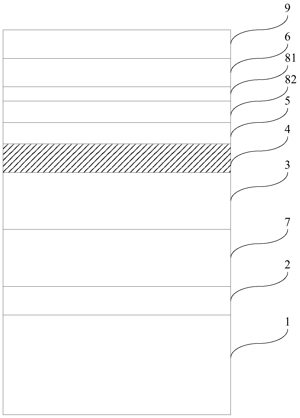
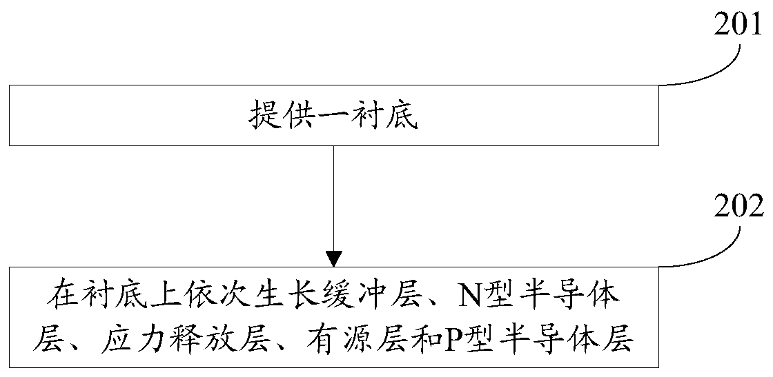
[0028] An embodiment of the present invention provides a light emitting diode epitaxial wafer. figure 1 A schematic structural diagram of a light emitting diode epitaxial wafer provided by an embodiment of the present invention. see figure 1 , the light-emitting diode epitaxial wafer includes a substrate 1, a buffer layer 2, an N-type semiconductor layer 3, a stress release layer 4, an active layer 5, and a P-type semiconductor layer 6, and the buffer layer 2, the N-type semiconductor layer 3, and the stress release layer 4. The active layer 5 and the P-type semiconductor layer 6 are sequentially stacked on the substrate 1 .

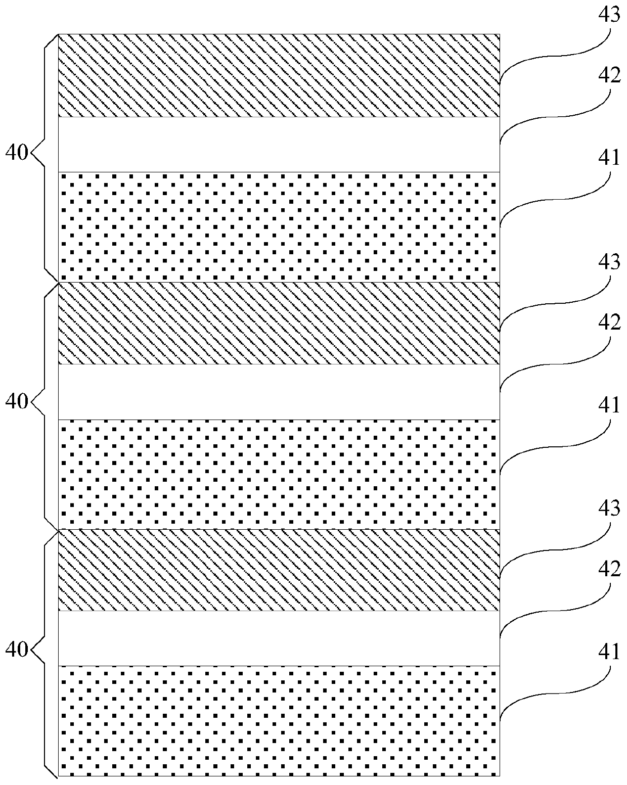
[0029] figure 2 Schematic diagram of the structure of the stress release layer provided by the embodiment ...


PUM


Abstract

The invention discloses a light-emitting diode epitaxial wafer and a growing method thereof and belongs to the field of semiconductor technology. The epitaxial wafer comprises a substrate, a buffer layer, an N-type semiconductor layer, a stress releasing layer, an active layer and a P-type semiconductor layer, wherein the buffer layer, the N-type semiconductor layer, the stress releasing layer, the active layer and the P-type semiconductor layer are sequentially stacked on the substrate; the stress releasing layer comprises multiple composite structures stacked sequentially, and each compositestructure comprises a first sub-layer, a second sub-layer and a third sub-layer stacked sequentially; the material of each first sub-layer is silicon and indium doped gallium nitride, the material ofeach second sub-layer is silicon-doped gallium nitride, and the material of each third sub-layer is indium-doped gallium nitride; and in the same composite structure, the doping concentration of silicon in the second sub-layer is smaller than the doping concentration of silicon in the first sub-layer, and the doping concentration of indium in the third sub-layer is greater than the doping concentration of indium in the first sub-layer. Through the light-emitting diode epitaxial wafer, the luminous efficiency of an LED can be improved.

Description

technical field [0001] The invention relates to the technical field of semiconductors, in particular to a light-emitting diode epitaxial wafer and a growth method thereof. Background technique [0002] Light Emitting Diode (English: Light Emitting Diode, referred to as: LED) is a semiconductor diode that can convert electrical energy into light energy. As an efficient, environmentally friendly, and green new solid-state lighting source, LEDs are rapidly and widely used in traffic lights, automotive interior and exterior lights, urban landscape lighting, mobile phone backlights and other fields. The core component of LED is the chip, and improving the luminous efficiency of the chip is the goal that is constantly pursued in the process of LED application. [0003] The chip includes an epitaxial wafer and electrodes provided on the epitaxial wafer. The existing LED epitaxial wafer includes a substrate, a buffer layer, an N-type semiconductor layer, an active layer and a P-ty...

Claims


Application Information

Patent Timeline
Patent Type & Authority Applications(China)
IPC IPC(8): H01L33/12H01L33/02H01L33/00
Inventor 从颖姚振胡加辉李鹏
Owner HC SEMITEK ZHEJIANG CO LTD
Why Eureka
Eureka Blog
Learn More