Method for covering thin film in hole and semiconductor processing apparatus

A technology for covering thin films and processing equipment, applied in semiconductor/solid-state device manufacturing, electrical components, circuits, etc., can solve the problems that TSV cannot achieve step coverage, reduce TSV step coverage, reduce film coverage, etc., and achieve the running direction. It is easier to control, take into account the production capacity, and reduce the effect of bombardment

Active Publication Date: 2019-06-14
BEIJING NAURA MICROELECTRONICS EQUIP CO LTD
View PDF5 Cites 3 Cited by
  • Summary
  • Abstract
  • Description
  • Claims
  • Application Information

AI Technical Summary

Problems solved by technology

If you continue to increase the RF bias power to make the metal ions gain more energy, the metal previously deposited at the bottom of the TSV will be more sputtered onto the sidewalls, resulting in a decrease in the film coverage at the bottom of the TSV and a reduction in the internal steps of the TSV. coverage
In addition, when the RF bias power is high, the deposition efficiency is low, which affects the productivity of the equipment
[0008] It can be seen from the above that using the standard cavity to process TSV with a large depth-to-width ratio cannot meet the requirements of step coverage, and the improved equipment has led to a decrease in the production capacity of the equipment, that is, the existing technology cannot achieve both process performance and production capacity.

Method used


Image

  • Method for covering thin film in hole and semiconductor processing apparatus
  • Method for covering thin film in hole and semiconductor processing apparatus
  • Method for covering thin film in hole and semiconductor processing apparatus

Examples


Embodiment Construction

[0034] In order for those skilled in the art to better understand the technical solution of the present invention, the method for covering a film in a hole and the semiconductor processing equipment provided by the present invention will be described in detail below with reference to the accompanying drawings.

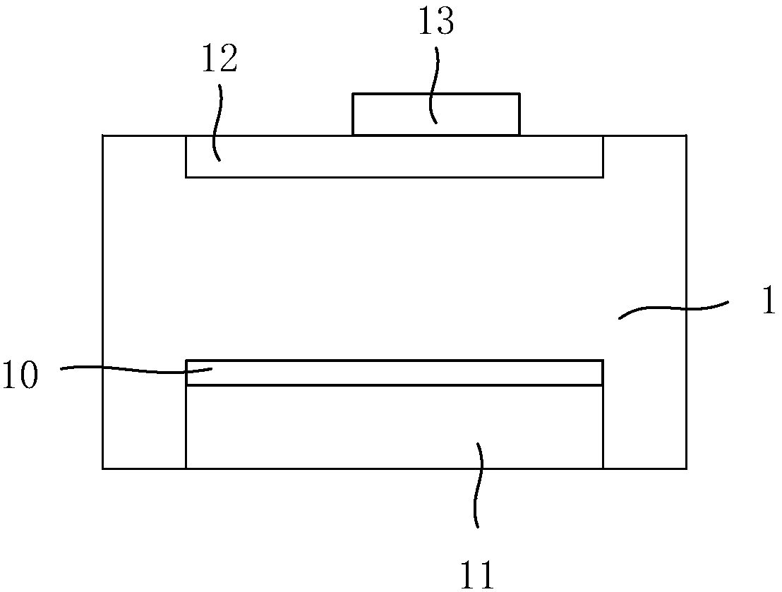
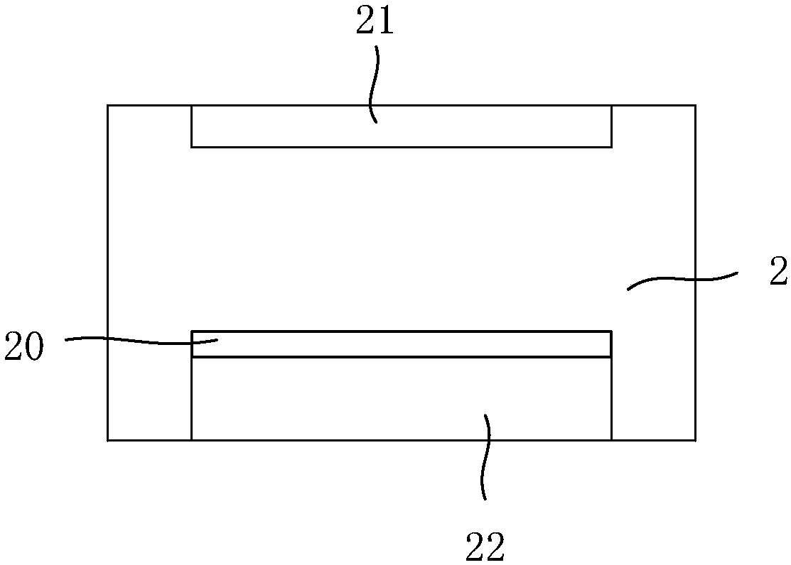
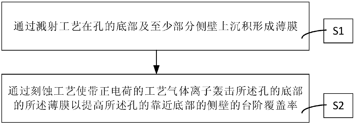
[0035] The semiconductor processing equipment provided by the present invention comprises a first chamber and a second chamber, the first chamber carries out a sputtering process, that is, the target metal ions obtained by the sputtering process in the first chamber, and the target metal ions Deposit and form a film on the bottom of the hole and at least part of the sidewall; the second chamber performs the reverse sputtering process, that is, the process gas is ionized in the second chamber, and the positively charged process gas ions are accelerated in the electric field The film is bombarded at the bottom of the well to increase the sidewall of the well near the bott...


PUM

PropertyMeasurementUnit
heightaaaaaaaaaa
heightaaaaaaaaaa

Abstract

The present invention provides a method for covering a thin film in a hole and a semiconductor processing apparatus. The method of covering a thin film in the hole comprises the following steps: step1, depositing a thin film on the bottom of the hole and at least a part of the sidewall by a sputtering process; and step 2, bombarding the positively charged process gas ions on the thin film at thebottom of the hole by an etching process to improve the step coverage of the sidewall near the bottom of the hole. The method of covering the film in the hole can not only improve the process performance, but also give consideration to the production capacity of the apparatus.

Description

technical field [0001] The invention belongs to the field of semiconductor manufacturing, and in particular relates to a method for increasing the step coverage in a hole and semiconductor processing equipment. Background technique [0002] With the improvement of integrated circuits, 3D packaging technology has become an important technical approach to realize high-density integrated circuits. Among them, Through Silicon Via (TSV) technology, as an important means of 3D packaging technology, has become more and more popular in the industry. Pay attention to. [0003] Generally, the TSV process includes photolithography, etching, chemical vapor deposition (CVD), physical vapor deposition (PVD) and electroplating in sequence. Among them, the physical vapor deposition process is used to realize the sputtering barrier layer and seed layer in the hole. The quality of this process has a great influence on the subsequent electroplating process. It is usually required that the bar...

Claims


Application Information

Patent Timeline
Patent Type & Authority Applications(China)
IPC IPC(8): H01L21/768H01L21/67
Inventor 卢平元侯珏杨敬山蒋秉轩王宽冒徐奎荣延栋
Owner BEIJING NAURA MICROELECTRONICS EQUIP CO LTD
Why Eureka
Try Eureka