High-stability OLED device and preparation method thereof

A high-stability, device technology, applied in the field of OLED devices, can solve problems such as pixel shrinkage, and achieve the effects of improving overlap, improving reliability, and avoiding electrochemical corrosion.

Inactive Publication Date: 2019-06-14
GUAN YEOLIGHT TECH CO LTD
View PDF0 Cites 11 Cited by
  • Summary
  • Abstract
  • Description
  • Claims
  • Application Information

AI Technical Summary

Problems solved by technology

[0005] Therefore, the technical problem to be solved by the present invention lies in the problem of pixel shrinkage caused by OUTGAS in the prior art. For this reason, the present invention provides a highly stable OLED device and its preparation method. By adding auxiliary electrodes, the brightness of the screen can be improved. Uniformity, and the Taper angle of the auxiliary electrode is 30-70°; at the same time, a pixel definition layer is arranged on the first electrode layer and the auxiliary electrode layer, which is in direct contact with the buffer layer, which is very good for OLED effective pixel area and / or pixel formation The surrounding structure prevents the release of volatile gas outgas into the pixel, causing the pixel to shrink, and improves the reliability of the OLED screen

Method used


Image

  • High-stability OLED device and preparation method thereof
  • High-stability OLED device and preparation method thereof
  • High-stability OLED device and preparation method thereof

Examples


preparation example Construction

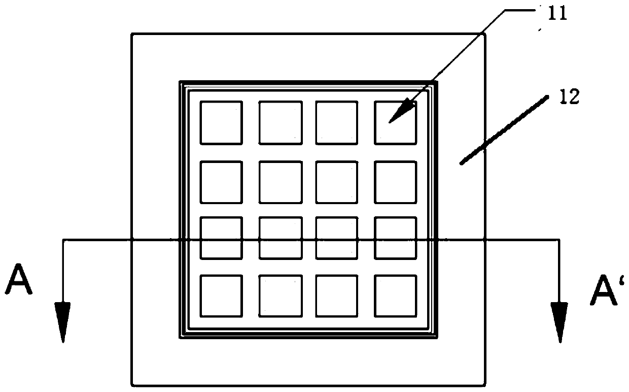
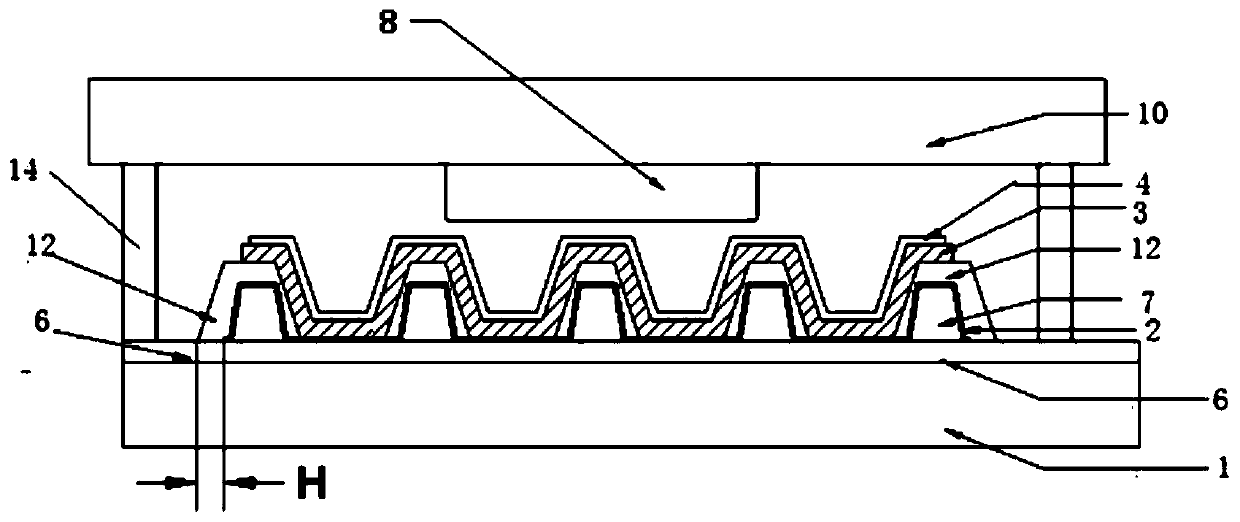
[0050] A preparation method of a highly stable OLED device, such as Figure 1 to Figure 2 shown, including the following steps:

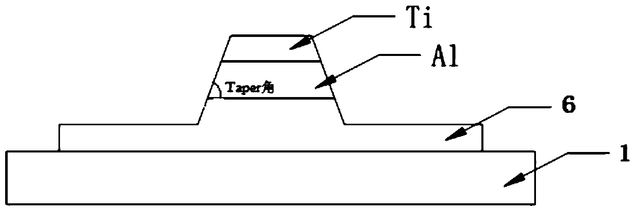
[0051] S1. Divide the pixel area 11 and the encapsulation area surrounding the pixel area 11 on the substrate 1, deposit a buffer layer 6 on the pixel area, prepare an auxiliary electrode layer on the buffer layer 6, and form several auxiliary electrode layers arranged at intervals by etching. The taper angle of the electrode 7 and the auxiliary electrode 7 is 30-70°;

[0052] S2. Prepare the first electrode layer 2 on the basis of step S1, the first electrode layer 2 covers the buffer layer 6 and the auxiliary electrode 7, and remove the first electrode layer between the auxiliary electrode 7 and the packaging area by etching An electrode layer 2 to expose the buffer layer 6;

[0053] S3. On the basis of step S2, deposit a pixel definition layer 12, the pixel definition layer 12 covers the first electrode layer 2 and the buffer layer 6 between th...

Embodiment 1

[0063] Such as figure 1 and figure 2 As shown, a highly stable OLED device provided by the present invention includes a substrate 1 and an encapsulation layer 10. The substrate 1 is divided into a pixel area 11 and an encapsulation area surrounding the pixel area 11. A sealing material layer 14 seals and connects the substrate 1 and the encapsulation layer 10 to form an airtight space. The side of the encapsulation layer close to the substrate 1 is provided with a drying sheet 8 to absorb moisture, and UV glue is used as the sealing material layer 14 to seal the substrate and the encapsulation layer. The packaging cover is used for packaging to improve the reliability of the screen packaging. The thickness of the buffer layer 6 is 50nm-500nm.

[0064] The light-emitting area of ​​the substrate 1 is provided with a buffer layer 6, and a plurality of auxiliary electrodes 7 arranged at intervals are arranged on the buffer layer 6, and the first electrode layer 2 covers the bu...

Embodiment 2

[0087] Such as Figure 5 and Figure 8 As shown, a kind of highly stable OLED device basic structure provided by the present invention is the same as embodiment 1, and its difference is:

[0088] The light-emitting area of ​​the substrate 1 is provided with a buffer layer 6, and the buffer layer 6 is provided with an anti-short circuit layer 13 formed by the first electrode layer, and several auxiliary electrodes 7 arranged at intervals, and the first electrode layer 2 covers The buffer layer 6 and the auxiliary electrode 7 are etched to remove the first electrode layer 2 located on one side or both sides of the auxiliary electrode 7, and the width of the first electrode layer 2 removed by etching is H=10um to expose the buffer layer 6;

[0089] Such as Figure 6 As shown, the pixel defining layer 12 completely covers the first electrode layer 2 on the auxiliary electrode and is provided with an opening exposing at least a part of the first electrode layer 2. The shape of th...


PUM


Abstract

The invention provides a high-stability OLED device and a preparation method thereof. The high-stability OLED device comprises a substrate and a packaging cover plate 10, wherein the substrate is divided into a pixel region and a packaging region; the substrate and the packaging cover plate are connected through a sealing medium; a first electrode layer, an organic light-emitting layer and a second electrode layer are overlapped on the pixel region on the substrate; and a buffer layer is arranged between the first electrode layer and the substrate. Through the arrangement of the buffer layer,the lateral erosion phenomenon caused by dry etching of the auxiliary electrode layer is solved, and meanwhile, metal ions of the glass substrate are blocked from permeating into the first electrode layer, and electrochemical corrosion is avoided; by adding the auxiliary electrode, the brightness uniformity of a screen body is improved; a pixel defining layer is simultaneously arranged on the first electrode layer and the auxiliary electrode layer and is in direct contact with the buffer layer, so that a very good surrounding structure is formed for an effective pixel region and/or pixels of the OLED, volatile gas outgas is prevented from being released into the pixels to cause pixel shrinkage, and the reliability of the screen body of the OLED is improved.

Description

technical field [0001] The invention relates to an OLED device, in particular to a highly stable OLED device and a preparation method. Background technique [0002] Organic light-emitting devices (English full name organic lighting emitting display, referred to as OLED) have the advantages of active light emission, wide color gamut, fast response, wide viewing angle, high contrast ratio, planarization, etc., and are the development trend of the next generation of display and lighting technology. [0003] An organic light emitting display device includes an anode layer, a light emitting layer and a cathode layer. Generally, there will be brightness unevenness in large-area lighting OLED light sources, and the brightness uniformity can be improved by adding auxiliary electrodes. However, the industry adopts dry etching method for etching, which is easy to produce Figure 4 Undercut, the main reason is that during the dry etching process, the dry etching gas is caused by the "...

Claims


Application Information

Patent Timeline
Patent Type & Authority Applications(China)
IPC IPC(8): H01L51/50H01L51/56H01L51/52
CPCH10K50/00H10K50/805H10K50/84H10K71/00H10K59/122H10K59/1795H10K59/173H10K59/1315H10K50/814H10K50/844H10K50/8426H10K59/1201H10K77/10H10K2102/00H10K2102/341H10K2102/351
Inventor 鲁天星吴海燕朱映光谢静张国辉胡永岚
Owner GUAN YEOLIGHT TECH CO LTD
Why Eureka
Try Eureka