A method for measuring trap states of gate dielectric layer for insulated gate type hemt

A technology of insulating gate type and gate dielectric layer, which is applied in the field of microelectronics, can solve the problems that the quality of the dielectric layer cannot be determined, and the extraction of the dielectric layer cannot be applied.

Active Publication Date: 2021-06-08
西安太乙电子有限公司
View PDF5 Cites 1 Cited by
  • Summary
  • Abstract
  • Description
  • Claims
  • Application Information

AI Technical Summary

Problems solved by technology

[0006] However, this method is only applied to HEMT devices, and cannot be applied to the extraction of the trap state density of the dielectric layer itself in MIS-HEMT devices, and the quality of the dielectric layer cannot be determined.

Method used


Image

  • A method for measuring trap states of gate dielectric layer for insulated gate type hemt
  • A method for measuring trap states of gate dielectric layer for insulated gate type hemt
  • A method for measuring trap states of gate dielectric layer for insulated gate type hemt

Examples


Embodiment Construction

[0066] DETAILED DESCRIPTION OF THE PREFERRED EMBODIMENTS An AlGaN / GaN heterojunction MIS-HEMT is taken as an example for illustration.

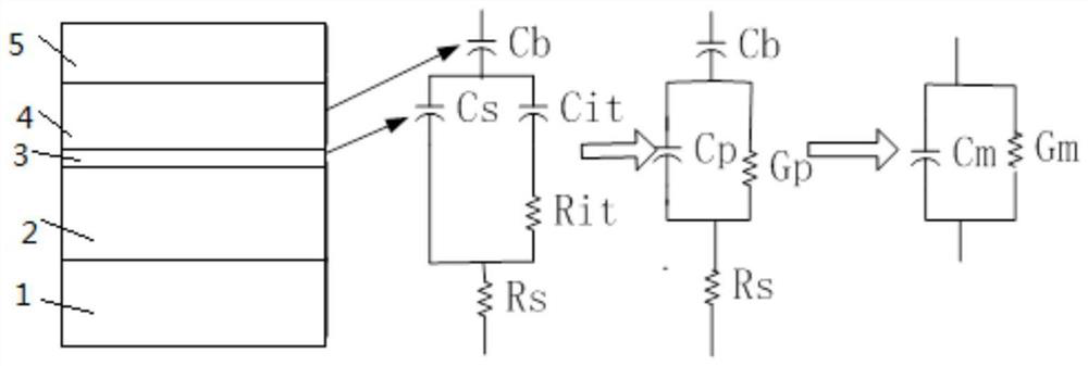
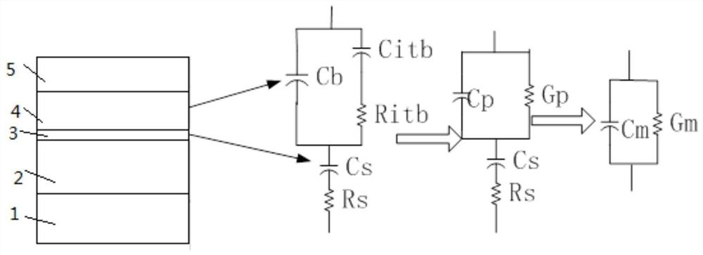
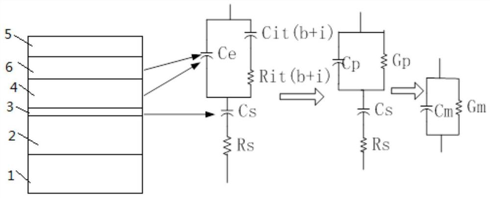
[0067] refer to figure 1 and figure 2 , the common HEMT structure used in the present invention, the structure is from bottom to top: substrate 1, transition layer 2, dielectric layer 3, barrier layer 4 and protection layer 5. refer to image 3 , The MIS-HEMT structure used in the present invention is as follows from bottom to top: substrate 1 , transition layer 2 , dielectric layer 3 , barrier layer 4 , insulating layer 6 and protection layer 5 .

[0068] The method for extracting the internal trap state of the gate dielectric layer in the present invention is as follows:

[0069] Step 1: Carry out the C-V characteristic test on the MIS-HEMT device and HEMT device used, obtain the corresponding C-V curve diagram, and determine the depletion voltage of the corresponding device according to the curve diagram; the C-V characteristic test cu...


PUM


Abstract

The invention discloses a method for measuring trap states in a gate dielectric layer of an insulated gate type HEMT. A masking method is used to manufacture HEMT devices on the same substrate, and corresponding devices are obtained by performing C-V characteristic tests on HEMT devices and MIS-HEMT devices. By selecting the gate voltage near the depletion voltage as the test point voltage, the characteristics of capacitance versus frequency (Cm~f) and conductance versus frequency (Gm~f) are tested under different grid voltages, and the general The trap state density of the barrier layer of the HEMT device and the total trap state density of the MIS-HEMT are calculated, and then the trap state density of the dielectric layer of the MIS-HEMT device is calculated, and the quality of the dielectric layer can be determined accordingly.

Description

technical field [0001] The invention belongs to the field of microelectronic technology, and relates to the problem of extracting the trap state density on the surface of semiconductor devices and gate dielectric layers, especially for high electron mobility transistors with heterojunction structures of III-V compound semiconductor materials, and can be used for such Comparative analysis of the trap state density of the device gate dielectric layer. Background technique [0002] Semiconductor materials composed of group III elements and group V elements, such as gallium nitride (GaN)-based, gallium arsenide (GaAs)-based semiconductor materials, often have large gap widths, so people usually use these III - Group V compound semiconductor materials form various heterojunction structures. The high electron mobility transistor based on the above heterojunction has the characteristics of high carrier mobility, high operating frequency, high power and good radiation resistance, a...

Claims


Application Information

Patent Timeline
Patent Type & Authority Patents(China)
IPC IPC(8): G01R31/26
Inventor 毕志伟张璨
Owner 西安太乙电子有限公司
Why Eureka
Try Eureka