Schottky field effect transistor based on silicon and transition metal sulfide and preparation method

A technology of transition metals and field effect transistors, which is applied in semiconductor/solid-state device manufacturing, semiconductor devices, electrical components, etc., can solve problems such as Fermi pinning, inability to form n-type contacts, and large contact resistance, so as to reduce Schott The effect of the base barrier

Active Publication Date: 2021-06-08
INST OF SEMICONDUCTORS - CHINESE ACAD OF SCI +1
View PDF2 Cites 0 Cited by
  • Summary
  • Abstract
  • Description
  • Claims
  • Application Information

AI Technical Summary

Problems solved by technology

[0004] In order to solve the problem of heterogeneous integration of transition metal sulfide contacts, at present, different types of metal and transition metal sulfide contacts are mainly used for research. Most metal and transition metal sulfide contacts are intrinsically n-type contacts, although theoretically the work function is relatively Low metal and transition metal sulfide contact will reduce the Schottky barrier, but because there are many interface states at the interface between metal and transition metal sulfide, it is easy to cause Fermi pinning, and metal and transition metal sulfide with different work functions Most of them cannot form a good n-type contact, and the Schottky barrier of the metal-transition metal sulfide system is relatively high, and the contact resistance is still relatively large, and there is no research report that the metal and transition metal sulfide will form a good contact. p-type Schottky barrier

Method used


Image

  • Schottky field effect transistor based on silicon and transition metal sulfide and preparation method
  • Schottky field effect transistor based on silicon and transition metal sulfide and preparation method
  • Schottky field effect transistor based on silicon and transition metal sulfide and preparation method

Examples


Embodiment Construction

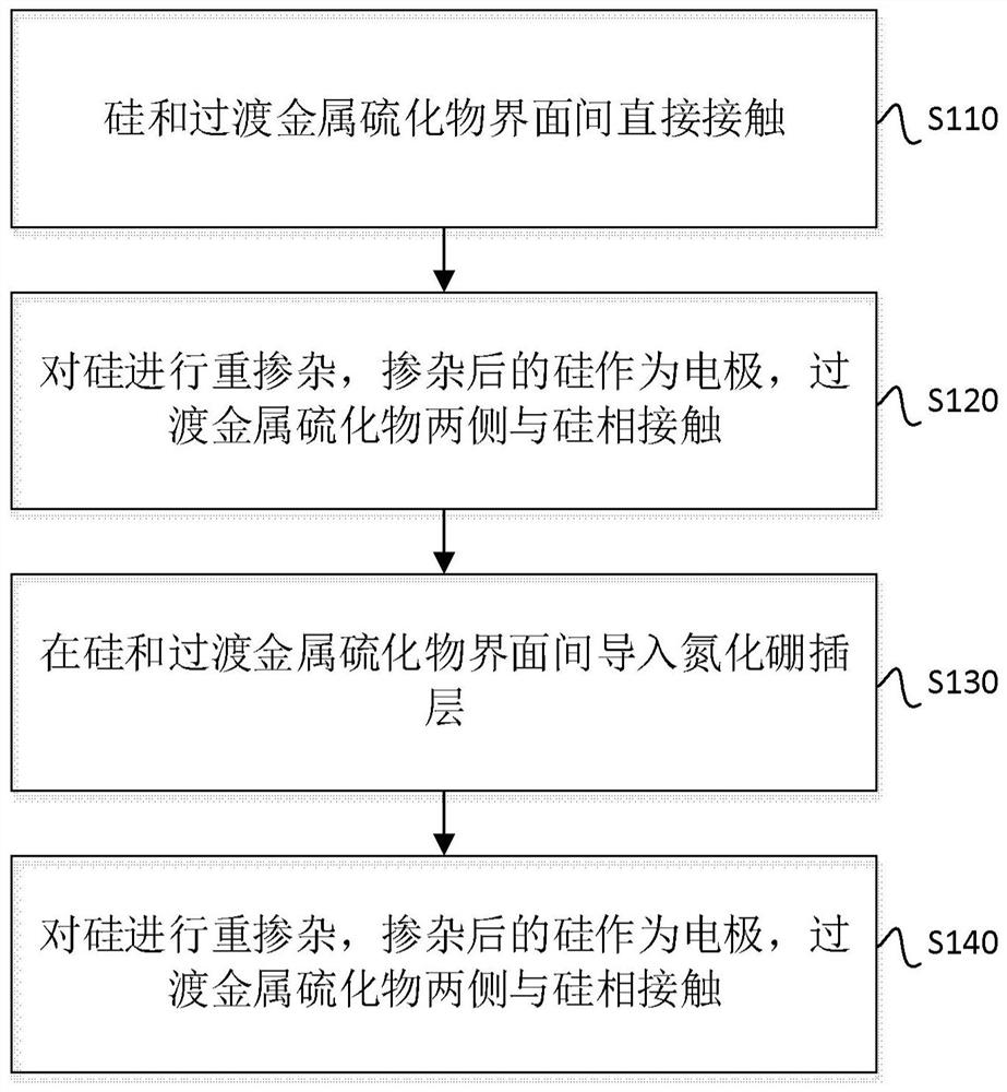
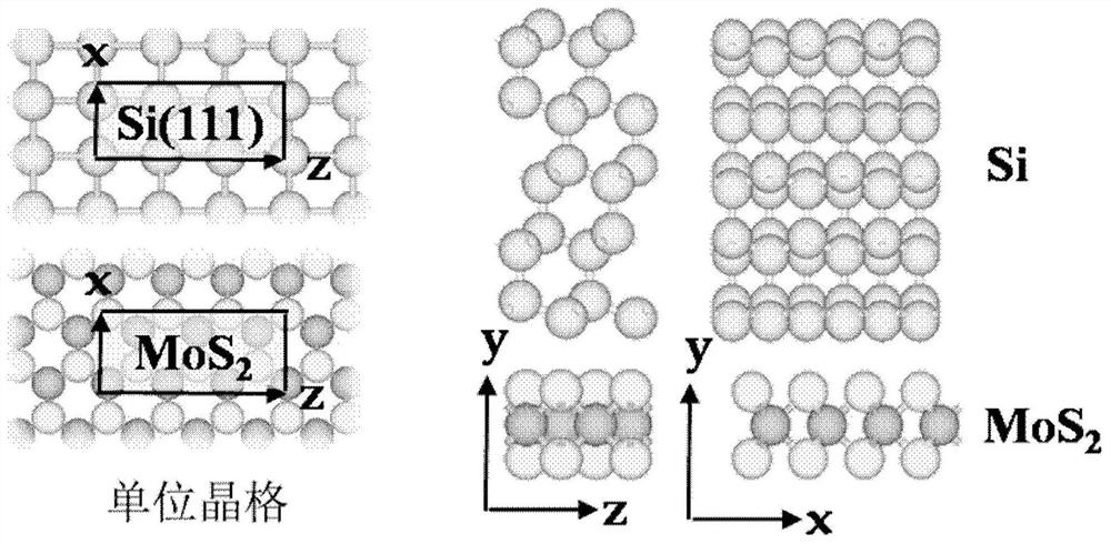
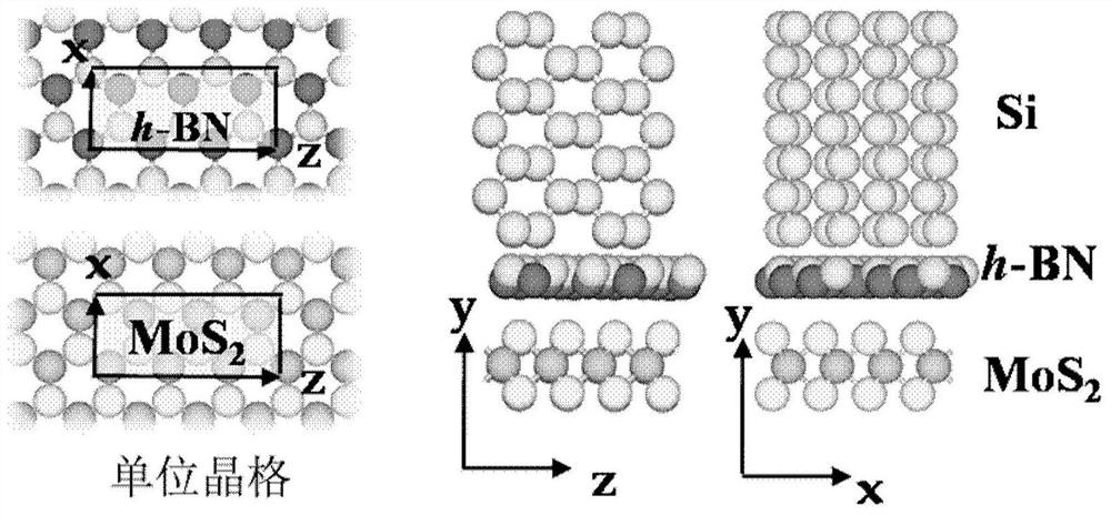
[0026] The disclosure provides a Schottky field effect transistor based on silicon and transition metal sulfide and its preparation method, the interface treatment method includes: introducing boron nitride intercalation between the interface of silicon and transition metal sulfide, Si as electrode, MoS 2 As a channel material, a PIP type Schottky field effect transistor is formed. The present disclosure is beneficial in reducing Si-MoS 2 The Schottky barrier of the system has great guiding significance for the integration of two-dimensional materials into traditional silicon materials in future microelectronic devices.

[0027] In order to make the purpose, technical solutions and advantages of the present disclosure clearer, the present disclosure will be further described in detail below in conjunction with specific embodiments and with reference to the accompanying drawings.

[0028] Certain embodiments of the present disclosure will be described more fully hereinafter w...


PUM


Abstract

The disclosure provides a Schottky field effect transistor based on silicon and transition metal sulfide and its preparation method, the interface treatment method includes: introducing boron nitride intercalation between the interface of silicon and transition metal sulfide, Si as electrode, MoS 2 As a channel material, a PIP type Schottky field effect transistor is formed. The present disclosure is beneficial in reducing Si-MoS 2 The Schottky barrier of the system has great guiding significance for the integration of two-dimensional materials into traditional silicon materials in future microelectronic devices.

Description

technical field [0001] The disclosure relates to the technical field of electronic devices, in particular to a Schottky field effect transistor based on silicon and transition metal sulfides and a preparation method. Background technique [0002] As traditional silicon-channel metal-oxide-semiconductor devices approach their scaling limits, alternative materials are needed in the post-silicon era. In the past decade, low-dimensional materials such as carbon nanotubes, graphene, and transition metal dichalcogenides (TMDs) have shown good electronic properties. Among various two-dimensional materials, they have fixed band gaps (1-2eV) and atomic-scale thickness Thin transition metal dichalcogenide semiconductors are considered to be the most promising candidates to replace silicon channels. And field-effect transistors based on single-layer transition metal dichalcogenides have been fabricated and intensively studied. [0003] When a metal and a semiconductor material are in...

Claims


Application Information

Patent Timeline
Patent Type & Authority Patents(China)
IPC IPC(8): H01L29/812H01L29/47H01L21/338
Inventor 姜向伟马晓雷陈杰智
Owner INST OF SEMICONDUCTORS - CHINESE ACAD OF SCI
Why Eureka
Try Eureka