Interface treatment method for reducing silicon and transition metal sulfide semiconductor schottky barrier

A technology of transition metal and Schottky potential, which is applied in semiconductor devices, semiconductor/solid-state device manufacturing, electrical components, etc., can solve the problems of interface state Fermi pinning and high contact Schottky barrier, and achieve low Schottky Effect of base barrier, low ohmic contact resistance

Inactive Publication Date: 2019-04-23
SHANDONG UNIV
View PDF4 Cites 0 Cited by
  • Summary
  • Abstract
  • Description
  • Claims
  • Application Information

AI Technical Summary

Problems solved by technology

[0005] The present invention aims at the problem of Fermi pinning caused by high contact Schottky barriers and interface states of existing metals and transition metal sulfides, and provides a method for reducing silicon and Transition Metal Chalcogenides Approach to Interfacial Schottky Barriers

Method used


Image

  • Interface treatment method for reducing silicon and transition metal sulfide semiconductor schottky barrier
  • Interface treatment method for reducing silicon and transition metal sulfide semiconductor schottky barrier
  • Interface treatment method for reducing silicon and transition metal sulfide semiconductor schottky barrier

Examples


Embodiment Construction

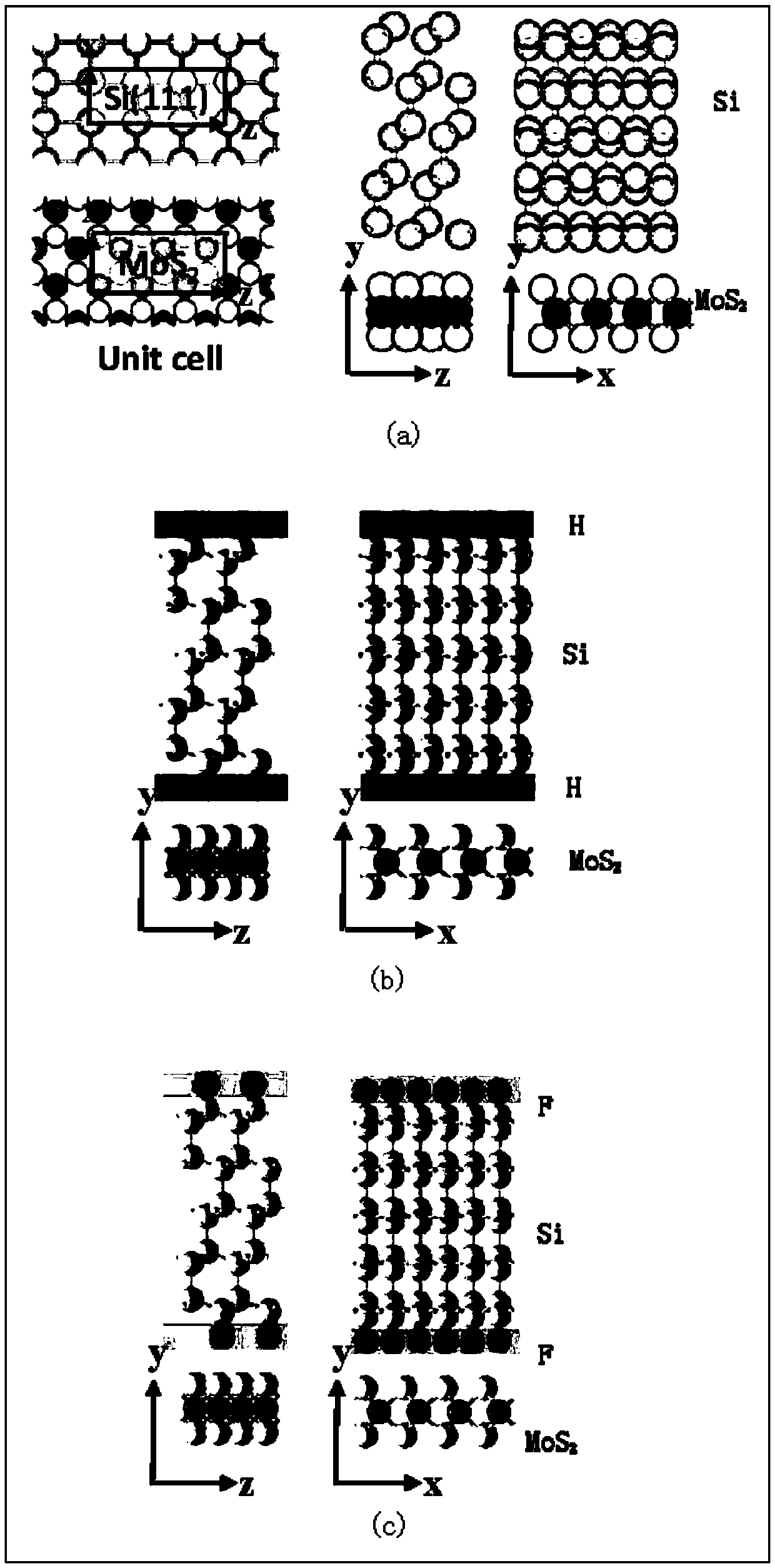
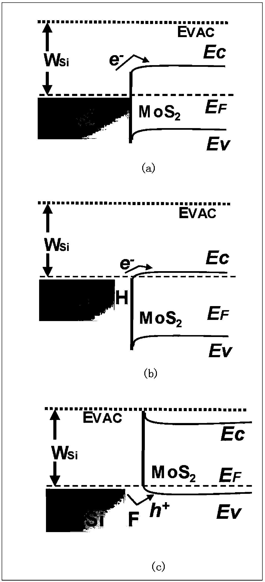
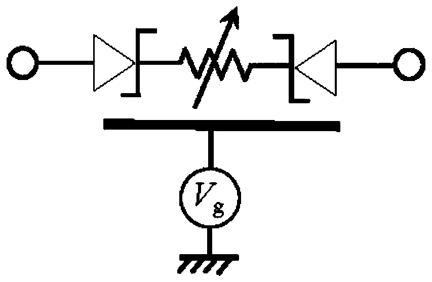
[0026] The method of the present invention to reduce the Schottky barrier of silicon and transition metal sulfide semiconductors is to passivate both the upper and lower surfaces of Si or only passivate the Si side close to the semiconductor surface, that is, through hydrogen or fluorine Surface passivation treatment is a well-known process for forming unsaturated Si bonds on the surface. After the surface of Si is passivated with hydrogen or fluorine, it can be in surface contact with both ends of the transition metal sulfide to form a NIN type Schottky field effect transistor and a PIP type Schottky field effect transistor respectively. Si-MoS passivated by hydrogen 2 system, the Si should be electronically doped. Si-MoS passivated by fluorine 2 system, hole doping is required for Si.

[0027] The method of the present invention will be further described in detail below by describing specific embodiments in conjunction with the accompanying drawings.

[0028] The interfa...


PUM


Abstract

The invention discloses an interface treatment method for reducing a silicon and transition metal sulfide semiconductor schottky barrier. Hydrogen or fluorine is used for conducting passivating treatment on the surface of Si, and then the Si and two ends of transition metal sulfide are subjected to surface contact to form an NIN-type schottky field-effect tube or a PIP-type schottky field-effect tube. According to a contact system after the hydrogen is used for passivating the Si surface, energy difference between a fermi level and a conduction band bottom of the transition metal sulfide is reduced so that the schottky barrier of the system can be reduced by passivating the Si surface through the hydrogen; secondly, the fluorine is used for passivating the Si surface, so that original n-type schottky contact can be turned into p-type schottky contact. According to the method, the traditional materials silicon and the transition metal sulfide are selected for surface contact, and through the traditional passivating element hydrogen or fluorine, the Si surface is subjected to passivating treatment so that the schottky barrier of the Si-MoS2 system can be reduced, and the interface treatment method for reducing the silicon and transition metal sulfide semiconductor schottky barrier has significant instructional significance for integration, of two-dimensional materials into the traditional silicon material, of microelectronic devices in the future.

Description

technical field [0001] The invention relates to an interface treatment method for Schottky barriers of silicon and transition metal sulfides, belonging to the technical field of electronic devices. Background technique [0002] As traditional silicon-channel metal-oxide-semiconductor devices approach their scaling limits, alternative materials are needed in the post-silicon era. In the past decade, low-dimensional materials such as carbon nanotubes, graphene, and transition metal sulfides have shown good electronic properties. Among various two-dimensional materials, transitions with fixed band gaps (1-2eV) and atomically thin Metal sulfide semiconductors are considered to be the most promising candidates to replace silicon channels. And field-effect transistors based on single-layer transition metal dichalcogenides have been fabricated and intensively studied. [0003] When a metal and a semiconductor material are in contact, the semiconductor energy band at the interface...

Claims


Application Information

Patent Timeline
Patent Type & Authority Applications(China)
IPC IPC(8): H01L21/335H01L29/812H01L29/267
CPCH01L29/267H01L29/66848H01L29/8126
Inventor 陈杰智马晓雷
Owner SHANDONG UNIV
Why Eureka
Try Eureka