Nige single crystal film with unlimited thickness and its preparation method and application

A single crystal thin film, limited technology, applied in semiconductor/solid-state device manufacturing, semiconductor devices, electrical components, etc., can solve the problems such as the difficulty of preparing single crystal thin films, and achieve good thermal stability, small contact resistance and low cost Effect

Active Publication Date: 2021-03-02
SOUTH UNIVERSITY OF SCIENCE AND TECHNOLOGY OF CHINA
View PDF5 Cites 0 Cited by
  • Summary
  • Abstract
  • Description
  • Claims
  • Application Information

AI Technical Summary

Problems solved by technology

The single crystal thin film prepared by this method aims to solve the problem that the single crystal thin film is difficult to prepare. This preparation method can alleviate the FLP effect at the NiGe-Ge interface, reduce the contact resistance of the NiGe-Ge junction, and improve the thermal stability of the NiGe thin film.

Method used


Image

  • Nige single crystal film with unlimited thickness and its preparation method and application
  • Nige single crystal film with unlimited thickness and its preparation method and application
  • Nige single crystal film with unlimited thickness and its preparation method and application

Examples


preparation example Construction

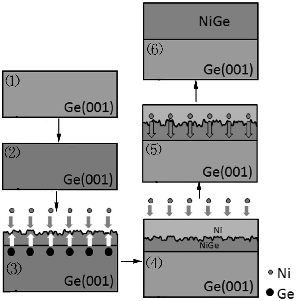
[0025] see figure 1 As shown in the preparation process flow chart, the embodiment of the present invention provides a method for preparing a NiGe single crystal thin film.

[0026] The preparation method comprises the following steps:

[0027] Step S01. Provide a clean Ge(001) substrate, such as figure 1 as shown in (1);

[0028] Step S02. Place the Ge(001) substrate in a vacuum environment for heat treatment, and then cool it down to room temperature to obtain a pre-used substrate, specifically as follows figure 1 as shown in (2);

[0029] Step S03. In a vacuum environment, carry out reactive evaporation treatment of Ni on the surface of the pre-used substrate, so that a layer of NiGe single crystal film is formed on the surface of Ge(001), specifically as follows figure 1 (3)~(4);

[0030] Step S04. At room temperature, vapor-deposit a layer of Ni film on the surface of the NiGe single crystal film, specifically as figure 1 (4)~(5);

[0031] Step S05. Under an inert ...

Embodiment 1

[0060] This embodiment 1 provides a method for preparing a NiGe single crystal thin film, comprising the following steps:

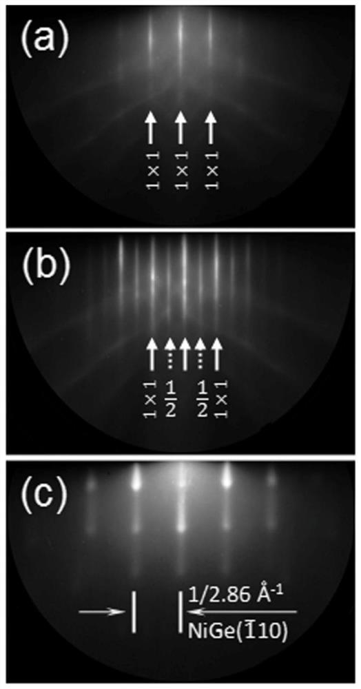
[0061] Step S11. Provide As-doped n-type Ge(001), whose volume resistivity is about 8Ωcm, and use it as a substrate, and perform a reflective high-energy electron diffraction (RHEED) scan on the Ge(001) substrate, and the specific results Such as figure 2 (a) shown.

[0062] Step S12. Cleaning Ge(001). Immerse the Ge(001) substrate in HF solution with a mass concentration of 1% for 1 min; take it out and soak it in flowing deionized water for 1 min, and immerse it in HF solution and deionized water 5 times in a cycle. ; followed by N 2 After drying the deionized water on the Ge(001) substrate with an air gun, immediately send the Ge(001) substrate into a chamber with a vacuum degree higher than 1e-5Pa, heat it to 700°C, keep the temperature constant for 60min, then cool it down to room temperature, and then Scan the RHEED graph, the specific results ...


PUM

PropertyMeasurementUnit
thicknessaaaaaaaaaa
thermal stabilityaaaaaaaaaa

Abstract

The invention relates to the technical field of semiconductor materials, and specifically provides a NiGe single crystal thin film and a preparation method and application thereof. The preparation method comprises the following steps: providing a clean Ge(001) substrate; heating the Ge(001) substrate in a vacuum to obtain a pre-used substrate; performing Ni reactive evaporation treatment on the pre-used substrate under vacuum, Form a layer of NiGe single crystal film on the surface of Ge(001); evaporate a layer of Ni film on the surface of NiGe single crystal film at room temperature; anneal the Ge(001) substrate in an inert atmosphere to make the Ni film diffuse A NiGe single crystal film is passed through, and the NiGe single crystal film is used as a single crystal seed layer, and a solid phase reaction occurs with a Ge(001) substrate to obtain a NiGe single crystal film with an unlimited thickness. The method can obtain NiGe single crystal film with low Schottky potential barrier, small contact resistance and good thermal stability, and is suitable for MOSFET field.

Description

technical field [0001] The invention belongs to the technical field of semiconductor materials, and in particular relates to a NiGe single crystal thin film with unlimited thickness, a preparation method and application thereof. Background technique [0002] Among many candidate channel materials, germanium has a hole mobility as high as 1900cm 2 / Vs is about 5 times that of the silicon channel material currently occupying a dominant position in the market. At the same time, the electron mobility of germanium is as high as 3900 cm 2 / Vs is about 2 times that of silicon. As a result, germanium-based metal-oxide-semiconductor field-effect transistors (Ge MOSFETs) have attracted widespread attention from researchers at home and abroad, and are considered to be important candidates for the next generation of ultra-high-speed and low-power large-scale integrated circuits. [0003] At present, the development of Ge MOSFETs still faces many problems, such as the short channel ef...

Claims


Application Information

Patent Timeline
Patent Type & Authority Patents(China)
IPC IPC(8): H01L21/02H01L29/78
CPCH01L21/02104H01L21/02631H01L29/78
Inventor 邓云生何东升邱杨顾瑞何佳清
Owner SOUTH UNIVERSITY OF SCIENCE AND TECHNOLOGY OF CHINA
Why Eureka
Try Eureka