Method for carrying out Fermi energy level modification on top electrode

A Fermi level and electrode technology, applied in circuits, electrical components, electrical solid devices, etc., can solve problems such as metal particle penetration, poor work function between electrodes and semiconductors, and changes in material properties

Active Publication Date: 2011-05-04
INST OF MICROELECTRONICS CHINESE ACAD OF SCI
View PDF4 Cites 0 Cited by
  • Summary
  • Abstract
  • Description
  • Claims
  • Application Information

AI Technical Summary

Problems solved by technology

However, there are also some problems in the device with the upper electrode structure. For example, when the electrode is evaporated, the metal particles will penetrate into the organic semiconductor material, and even the organic semiconductor material will undergo a chemical reaction to change the performance of the material; another example is the difference between the work function of the electrode material and the organic semiconductor material. Schottky barrier caused by mismatch, etc.
[0004] At present, in order to overcome the problem of metal penetration into the semiconductor, the general solution is to add an organic barrier layer under the electrode, but there has been no good solution to the problem of the work function difference between the electrode and the semiconductor.

Method used


Image

  • Method for carrying out Fermi energy level modification on top electrode
  • Method for carrying out Fermi energy level modification on top electrode
  • Method for carrying out Fermi energy level modification on top electrode

Examples


Embodiment Construction

[0025] In order to make the object, technical solution and advantages of the present invention clearer, the present invention will be described in further detail below in conjunction with specific embodiments and with reference to the accompanying drawings.

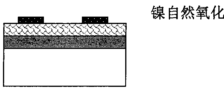
[0026] The method for modifying the Fermi level of the upper electrode provided by the present invention is to steam a thin layer of metal nickel before steaming a metal electrode, especially a gold electrode, and then take it out and expose it to the air to allow the nickel to oxidize naturally to form A thin layer of nickel oxide with a relatively high Fermi energy level, and finally a layer of metal layer is evaporated to form the upper electrode.

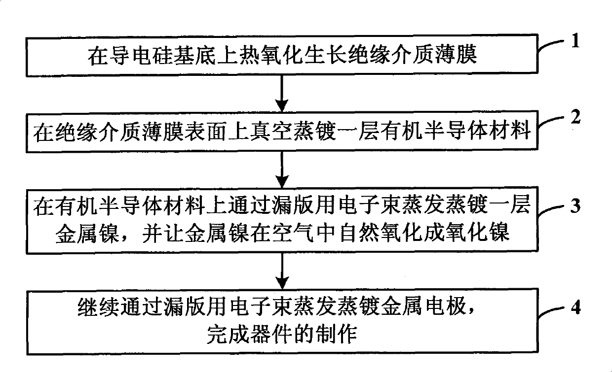
[0027] Such as figure 1 as shown, figure 1 It is a flow chart of a method for modifying the upper electrode at the Fermi level provided by the present invention, and the method includes:

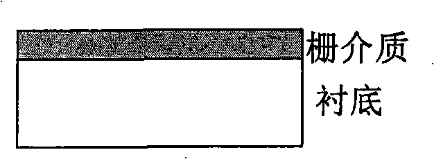
[0028] Step 1, thermally oxidize and grow an insulating dielectric film on a conduc...


PUM

PropertyMeasurementUnit
thicknessaaaaaaaaaa
thicknessaaaaaaaaaa

Abstract

The invention discloses a method for carrying out Fermi energy level modification on a top electrode, which comprises the following steps: step 1) carrying out thermal oxidation growth of an insulation dielectric thin film on a conductive silicon substrate; step 2) carrying out vacuum evaporation of a layer of organic semiconductor material on the surface of the insulation dielectric thin film; step 3) using electron beam evaporation for evaporating a layer of metal nickel on the organic semiconductor material through a stencil, and naturally oxidizing the metal nickel to nickel oxide in the air; and step 4) continuously using the electron beam evaporation for evaporating a metal electrode through the stencil and completing the production of a device. The utilization of the method can effectively reduce the infiltration and the reaction of a gold electrode to the organic semiconductor layer; simultaneously, the naturally oxidized nickel oxide layer can be taken as a high-work-functiontransition layer, thereby reducing the Schottky barrier between the gold electrode and the organic semiconductor layer and further improving the contact between the electrode and an active layer.

Description

technical field [0001] The invention relates to the technical field of microfabrication in organic semiconductors, in particular to a method for modifying the upper electrode at the Fermi level in the process of manufacturing an organic field effect transistor with an upper electrode structure. Background technique [0002] With the continuous deepening of information technology, electronic products have entered every aspect of people's life and work; in daily life, people's demand for low-cost, flexible, low-weight, and portable electronic products is increasing; traditional inorganic semiconductor-based It is difficult for devices and circuits of materials to meet these requirements, so organic microelectronics technology based on organic polymer semiconductor materials that can realize these characteristics has received more and more attention under this trend. [0003] Improving the performance of organic field effect transistors has always been a goal pursued by this fi...

Claims


Application Information

Patent Timeline
Patent Type & Authority Patents(China)
IPC IPC(8): H01L51/40H01L51/10H01L21/28
Inventor 刘舸刘明刘兴华商立伟王宏柳江
Owner INST OF MICROELECTRONICS CHINESE ACAD OF SCI
Why Eureka
Try Eureka