A lumped parameter ipd broadband coupler
A lumped parameter, coupler technology, applied in the field of electronics, can solve problems such as size increase, disadvantageous device or integrated circuit miniaturization, etc., and achieve the effect of low insertion loss, high cost performance and high cost performance
- Summary
- Abstract
- Description
- Claims
- Application Information
AI Technical Summary
Problems solved by technology
Method used
Image
Examples
Embodiment Construction
[0023] The present invention will be described in detail below in conjunction with the accompanying drawings.
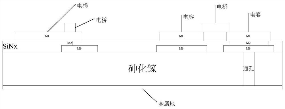
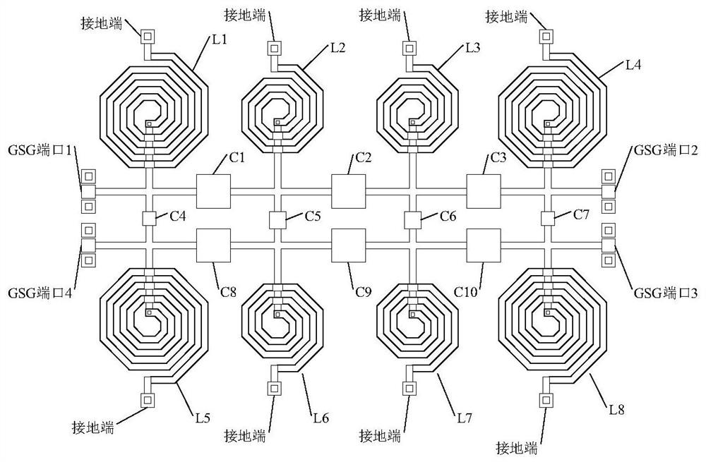
[0024] Such as figure 1 , the lumped parameter broadband coupler of the present invention includes a ground metal layer, a substrate, a dielectric layer and an LC broadband coupler. The substrate is a gallium arsenide substrate, and the dielectric layer is a SiNx substrate. The ground metal layer is located on the lower surface of the substrate and is connected to the LC broadband coupler through the TGV gallium through hole in the substrate. The dielectric layer is located on the upper surface of the substrate. The LC broadband coupler is distributed in three metal layers M1, M2 and M3, the first metal layer M1 is arranged above the upper surface of the dielectric layer, and the second metal layer M2 and the third metal layer M3 are integrated in the dielectric layer Among them, the third metal layer M3 is close to the upper surface of the substrate, and the seco...
PUM
| Property | Measurement | Unit |
|---|---|---|
| frequency | aaaaa | aaaaa |
Abstract
Description
Claims
Application Information


