Two-dimensional optical grating-based light absorber and manufacturing method thereof

A two-dimensional grating and manufacturing method technology, applied in optics, instruments, optical components, etc., can solve problems such as difficult graphics, and achieve the effects of suppressing sensitivity, high-efficiency absorption, and good stability

Inactive Publication Date: 2019-06-25
HUBEI UNIV
View PDF5 Cites 6 Cited by
  • Summary
  • Abstract
  • Description
  • Claims
  • Application Information

AI Technical Summary

Problems solved by technology

At present, most of the researches are concentrated in the infrared band, and there are few studies in the visible band. However, in the visible wavelength range, the sub-wavelength metal nanostructures exhibit unique optical properties due to the remarkable surface plasmon effect. The energy of these resonances is largely Depends on the shape, size and material characteristics of material particles, but it is only limited to theoretical research at present, this is because it is very difficult to prepare nano-sized patterns in practice, and the present invention is to solve the problem of preparing devices in practice

Method used


Image

  • Two-dimensional optical grating-based light absorber and manufacturing method thereof
  • Two-dimensional optical grating-based light absorber and manufacturing method thereof
  • Two-dimensional optical grating-based light absorber and manufacturing method thereof

Examples


Embodiment 1

[0027] A: Place silicon wafers in acetone, absolute ethanol (wt99.99, AR) and deionized water for ultrasonic cleaning for 30 minutes, blow dry with a nitrogen gun, then dry with a drying table higher than 100°C, and cool for 3 minutes;

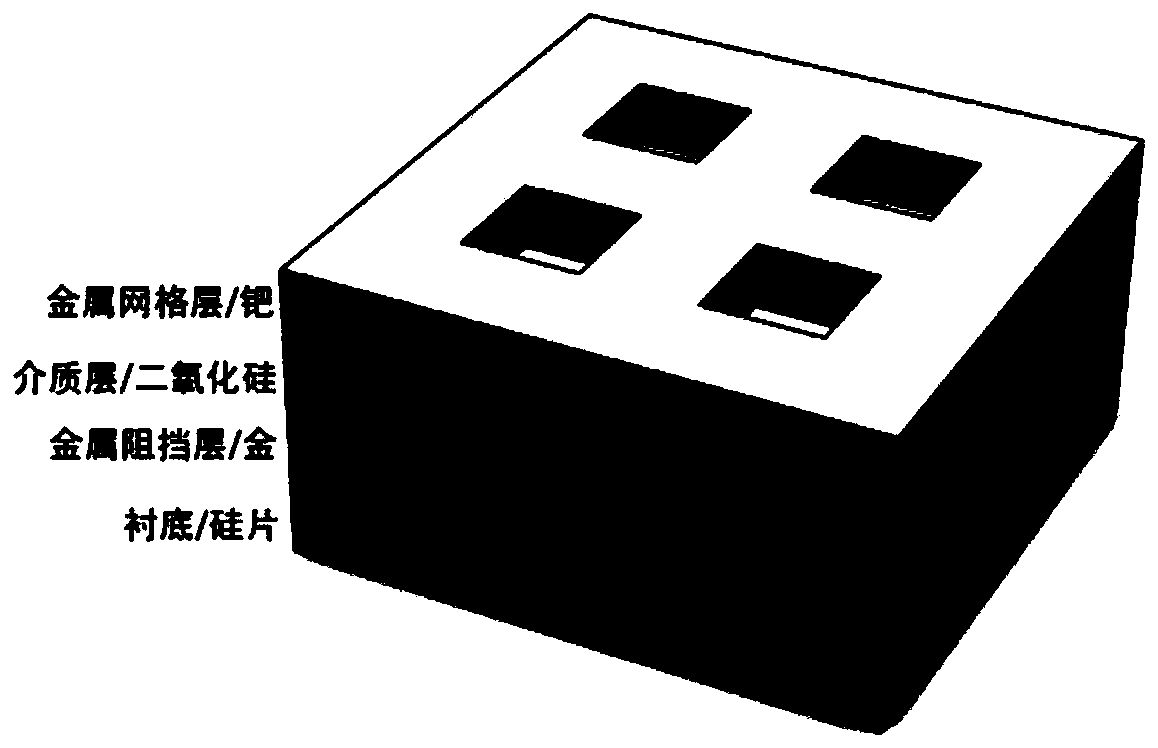
[0028] B: Use DC sputtering process to sputter a layer of Cr on the silicon wafer as the connecting metal, pump for 6 hours, and the vacuum degree is lower than 5×10 -4 Pa, the sputtering power is 100w, the sputtering pressure is 0.5Pa, the sputtering time is 4s, and then a layer of Au is sputtered by DC sputtering process, and the vacuum is lower than 5×10 -4 Pa, the sputtering power is 100w, the sputtering pressure is 0.5Pa, the sputtering time is 25s, and then a layer of SiO is sputtered by radio frequency sputtering process 2 , pumping for 6h, the vacuum degree is lower than 5×10 -4 Pa, the RF sputtering power is 100w, the sputtering pressure is 0.5Pa, and the sputtering time is 15s;

[0029]C: A layer of MMA is spin-coated on the sputte...

Embodiment 2

[0035] A: Place silicon wafers in acetone, absolute ethanol (wt99.99, AR) and deionized water for ultrasonic cleaning for 30 minutes, blow dry with a nitrogen gun, then dry with a drying table higher than 100°C, and cool for 3 minutes;

[0036] B: Use DC sputtering process to sputter a layer of Cr on the silicon wafer as the connecting metal, pump for 6 hours, and the vacuum degree is lower than 5×10 -4 Pa, the sputtering power is 100w, the sputtering pressure is 0.5Pa, the sputtering time is 4s, and then a layer of Au is sputtered by DC sputtering process, and the vacuum is lower than 5×10 -4 Pa, the sputtering power is 100w, the sputtering pressure is 0.5Pa, the sputtering time is 25s, and then a layer of SiO is sputtered by radio frequency sputtering process 2 , pumping for 6h, the vacuum degree is lower than 5×10 -4 Pa, the RF sputtering power is 100w, the sputtering pressure is 0.5Pa, and the sputtering time is 15s;

[0037] C: A layer of MMA is spin-coated on the sputt...

Embodiment 3

[0043] A: Place silicon wafers in acetone, absolute ethanol (wt99.99, AR) and deionized water for ultrasonic cleaning for 30 minutes, blow dry with a nitrogen gun, then dry with a drying table higher than 100°C, and cool for 3 minutes;

[0044] B: Use DC sputtering process to sputter a layer of Cr on the silicon wafer as the connecting metal, pump for 6 hours, and the vacuum degree is lower than 5×10 -4 Pa, the sputtering power is 100w, the sputtering pressure is 0.5Pa, the sputtering time is 4s, and then a layer of Au is sputtered by DC sputtering process, and the vacuum is lower than 5×10 -4 Pa, the sputtering power is 100w, the sputtering pressure is 0.5Pa, the sputtering time is 25s, and then a layer of SiO is sputtered by radio frequency sputtering process 2 , pumping for 6h, the vacuum degree is lower than 5×10 -4 Pa, the RF sputtering power is 100w, the sputtering pressure is 0.5Pa, and the sputtering time is 15s;

[0045] C: A layer of MMA is spin-coated on the sputt...


PUM


Abstract

The invention discloses a two-dimensional optical grating-based light absorber and a manufacturing method thereof. With the two-dimensional optical grating-based light absorber and the manufacturing method thereof of the invention adopted, high-efficiency absorption of external incident light in different frequency bands can be realized. The light absorbing structure comprises a metal mesh layer,a dielectric layer, a metal barrier layer and a substrate which are sequentially distributed from top to bottom; the metal barrier layer satisfies the excitation of a surface plasmons effect by incident light on the surface of the dielectric layer; the incident light radiates at the interface of the metal mesh layer and the dielectric layer so as to form surface plasmons; the two kinds of plasmonswhich are spatially separated from each other are subjected to symmetric plasmon coupling in the dielectric layer. The light absorber of the invention has high efficiency absorption for different visible light bands, and can greatly suppress the sensitivity of light absorption characteristics to the incident angle of the incident light.

Description

technical field [0001] The invention belongs to the technical field of electromagnetic protection, and relates to a light absorber structure and production, in particular to a two-dimensional grating-based light absorber and a production method thereof. Background technique [0002] Artificial electromagnetic metamaterials refer to a new type of composite artificial materials whose dielectric constant ε and magnetic permeability μ can be controlled artificially, and the parameters of the two parameters can be positive or negative. Artificial electromagnetic metamaterials exhibit electromagnetic responses that do not exist in natural materials, such as negative refractive index, artificial magnetic response, hyperfocus, etc. Another advantage of electromagnetic metamaterials is that resonant structures can be designed in a wide range, from radio frequency bands to terahertz bands and to infrared bands. At present, the metamaterial plasmonic structure exhibits greater absorpt...

Claims


Application Information

Patent Timeline
IPC IPC(8): G02B5/00
Inventor 顾豪爽余念王钊胡永明熊娟
Owner HUBEI UNIV
Why Eureka
Try Eureka