Semiconductor structures and methods of forming them

A semiconductor and conductive structure technology, applied in the field of semiconductor structure and its formation, can solve the problems of MOSFET performance to be improved, and achieve the effect of increasing size, reducing loss and improving performance

Active Publication Date: 2021-12-14
SEMICON MFG INT (SHANGHAI) CORP +1
View PDF5 Cites 0 Cited by
  • Summary
  • Abstract
  • Description
  • Claims
  • Application Information

AI Technical Summary

Problems solved by technology

[0004] However, the performance of the MOSFET with the vertical all-around gate structure in the prior art needs to be improved

Method used


Image

  • Semiconductor structures and methods of forming them
  • Semiconductor structures and methods of forming them
  • Semiconductor structures and methods of forming them

Examples


Embodiment Construction

[0032] There are many problems in the semiconductor structure in the prior art, for example, the performance of the formed semiconductor structure is poor.

[0033] Combining with a semiconductor structure, the reason for the poor performance of the existing semiconductor structure is analyzed:

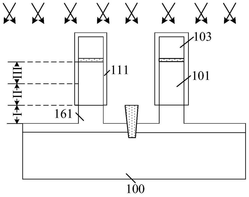
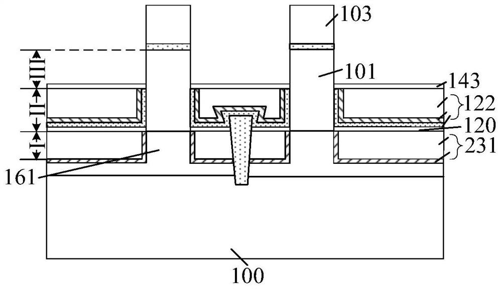
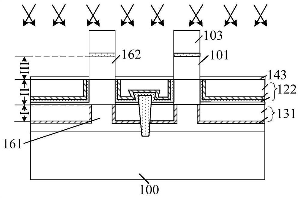
[0034] Figure 1 to Figure 3 It is a structural schematic diagram of each step of a method for forming a semiconductor structure.

[0035] Please refer to figure 1 , providing a substrate 100 having a fin post 101 thereon, the fin post 101 comprising a bottom region I; a channel region II located on the bottom region I; a channel region II located on the channel region II The top region III of the fin pillar 201 has a mask layer 203 on it.

[0036] continue to refer figure 1 , forming a sidewall 111 covering the top region III and the channel region II of the fin column 101; using the sidewall 111 as a mask to perform the first ion implantation on the fin column 101, in the fin c...


PUM

PropertyMeasurementUnit
sizeaaaaaaaaaa
thicknessaaaaaaaaaa
heightaaaaaaaaaa

Abstract

A semiconductor structure and its forming method, wherein, the forming method includes: providing a substrate with a sacrificial column on the substrate; forming a supporting structure on the gate, the supporting structure exposing the sacrificial column top; after the support structure is formed, the sacrificial column is removed, a first opening is formed in the first conductive structure, a second opening is formed in the gate, and a third opening is formed in the support structure; forming a first doped layer in an opening, and doping first doped ions into the first doped layer through first in-situ doping; forming a channel layer in the second opening; A second doping layer is formed in the third opening, and second doping ions are doped into the second doping layer through second in-situ doping. The formation method can improve the performance of the semiconductor structure.

Description

technical field [0001] The invention relates to the technical field of semiconductor manufacturing, in particular to a semiconductor structure and a forming method thereof. Background technique [0002] Metal-oxide-semiconductor field-effect transistors (MOSFETs) are among the most important components in modern integrated circuits. With the development of semiconductor technology, the traditional planar MOSFET's ability to control the channel current becomes weaker, resulting in serious leakage current. Fin field effect transistor (Fin FET) is an emerging multi-gate device, which generally includes a fin protruding from the surface of the semiconductor substrate, a gate covering part of the top surface and side walls of the fin, and a gate located on the gate. The source and drain doped regions in the fins on both sides of the pole. Compared with the planar MOSFET, the fin field effect transistor has a stronger short-channel suppression ability and a stronger working curr...

Claims


Application Information

Patent Timeline
Patent Type & Authority Patents(China)
IPC IPC(8): H01L21/336H01L29/78H01L29/06
Inventor 李勇洪中山
Owner SEMICON MFG INT (SHANGHAI) CORP
Why Eureka
Try Eureka