A method for improving the gate metal/semiconductor interface of gan devices
A gate metal and semiconductor technology, applied in the field of microelectronics, can solve the problems of restricting the actual use of devices, lack of GaN device gate metal/semiconductor interface characteristics, and affecting the normal operation of devices, so as to improve the interface quality, enhance the degree of improvement, and reliability Enhanced effect
- Summary
- Abstract
- Description
- Claims
- Application Information
AI Technical Summary
Problems solved by technology
Method used
Image

Examples
Embodiment 1
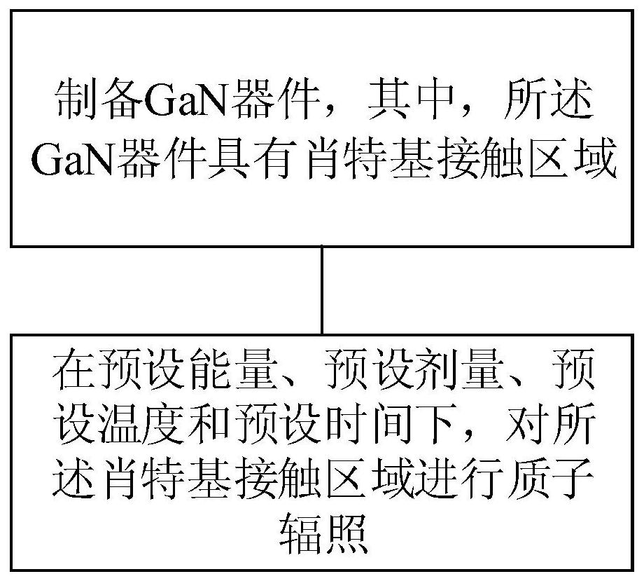
[0035] See figure 1 , figure 1 A schematic flowchart of a method for improving the gate metal / semiconductor interface of a GaN device provided by an embodiment of the present invention, including:
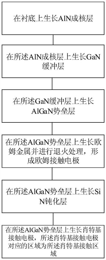
[0036] S1. Prepare a GaN device, wherein the GaN device has a Schottky contact region; please refer to figure 2 , figure 2 A schematic flow diagram for preparing a GaN device provided by an embodiment of the present invention, specifically including steps:
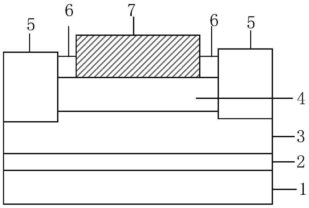
[0037] S11, selecting a substrate 1;
[0038] Sapphire is selected as the substrate of the AlGaN / GaN epitaxial structure. The reason for using sapphire as the substrate is that there is no economically available natural substrate for GaN. The growth of GaN can only be epitaxy through some heterogeneous substrates, and GaN is grown on the sapphire substrate. , the defects caused by lattice mismatch are smaller than other substrates, and the price of sapphire is lower.
[0039] S12, growing an AlN nucleation layer 2 on the...
Embodiment 2
[0066] Firstly, the first GaN device is prepared, and the steps of preparing the first GaN device are as described in the first embodiment.
[0067] Then, a semiconductor parameter analyzer is used to perform capacitance-voltage (C-V) tests at multiple frequencies (10kHz-5MHz) on the first GaN device, and the first data is obtained as the data of the initial state; wherein, the gate voltage during the C-V test is set to -6V to 1V.
[0068] Secondly, at the preset energy of 3 MeV and the first dose of 5×10 13 h + / cm 2 1. Under the conditions of a preset temperature of 22° C. (room temperature) and a vacuum environment, a low-energy accelerator is used to uniformly irradiate the Schottky contact region of the first GaN device with an irradiation time of 10 h.
[0069] Then after the irradiation is completed, a semiconductor parameter analyzer is used to perform capacitance-voltage (C-V) tests on the irradiated GaN device at multiple frequencies (10kHz-5MHz), and the second d...
Embodiment 3
[0087] On the basis of Example 2, first prepare the second GaN device, the steps of preparing the second GaN device are the same as preparing the first GaN device; then carry out C-V test, proton irradiation, C-V test and physical parameter extraction on the second GaN device For the process of C-V test, proton irradiation, and physical parameter extraction process, please refer to Example 2. During proton irradiation, the second dose is 1×10 14 h + / cm 2 The second device is irradiated.
[0088] Next, prepare the third GaN device, the steps of preparing the third GaN device are the same as preparing the first GaN device; then carry out the process of C-V test, proton irradiation, C-V test and physical parameter extraction on the third GaN device, wherein, the C-V test , proton irradiation, physical parameter extraction process please refer to embodiment two, the third dose is 5 × 10 14 h + / cm 2 The third device is irradiated.
[0089] See Figure 6 , Figure 6 A comp...
PUM
 Abstract
Description
Claims
Application Information