
CMOS combination logic circuit

A combinatorial logic circuit, low-level technology, applied to logic circuits with logic functions, etc., can solve problems such as difficulty in meeting server performance requirements

Pending Publication Date: 2019-07-02
深圳市致宸信息科技有限公司
View PDF0 Cites 0 Cited by
  • Summary
  • Abstract
  • Description
  • Claims
  • Application Information

AI Technical Summary

Problems solved by technology

When the high-performance computing server is very sensitive to power consumption and speed, it is difficult to meet the performance requirements of the server with such a tool processing method, so designers need some low-power consumption or speed-up logic cells to replace the combination in the standard cell library logic operation unit circuit, which reduces power consumption and increases speed

Method used


Image

  • CMOS combination logic circuit
  • CMOS combination logic circuit
  • CMOS combination logic circuit

Examples


Embodiment Construction

[0021] The technical solutions in the embodiments of the present invention will be clearly and completely described below with reference to the accompanying drawings in the embodiments of the present invention. Obviously, the described embodiments are only a part of the embodiments of the present invention, but not all of the embodiments.

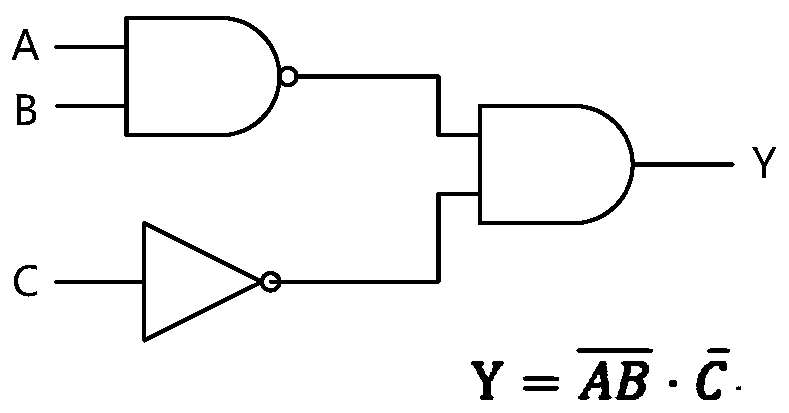
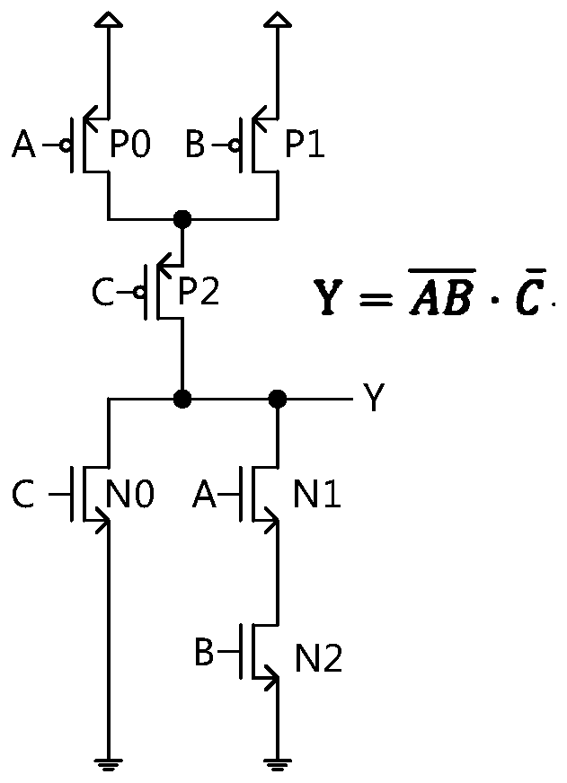
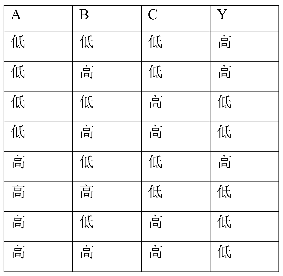
[0022] like figure 1 As shown, the present invention provides a circuit unit structure that realizes Logical operation function.

[0023] In the PMOS network, the first transistor, the second transistor and the third transistor are all PMOS transistors. The gate G of the first transistor P0 is connected to the first input signal A, the source S is connected to the power supply voltage VDD, the drain D is connected to the drain D of the second transistor P1 and the source S of the third transistor P2; The gate G of the transistor P1 is connected to the second input signal B, the source S is connected to the power supply voltage VDD, and t...


PUM


Abstract

The invention provides a CMOS (Complementary Metal-Oxide-Semiconductor Transistor) combinational logic circuit, which is used for replacing a combinational logic operation unit circuit in a standard unit library provided by a process plant when an adder circuit is designed. The CMOS combination logic circuit comprises a PMOS network and an NMOS network, wherein the PMOS network and the NMOS network respectively comprise three transistors. The logic operation function is realized through fewer transistors, the area is reduced, the power consumption is reduced, meanwhile, the path is shortened,and the transmission delay is reduced.

Description

technical field [0001] The invention relates to a circuit unit structure, in particular to a small CMOS combinational logic operation unit circuit for replacing the combinational logic operation unit circuit in a standard cell library provided by a process factory. Background technique [0002] When designing the core chip in a large-scale high-performance computing server, in the current design process, from the front-end RTL (resistor transistor logic circuit) design to the back-end implementation, all are based on the standard cell library provided by the process factory. Although the design cycle is short, But the available resources are limited (only the standard cell library provided by the process factory) and lack flexibility. When high-performance computing servers are sensitive to power consumption and speed, it is difficult to meet the performance requirements of the server with such a tool processing method, so designers need some low-power or speed-up logic cell...

Claims


Application Information

Patent Timeline
IPC IPC(8): H03K19/20
CPCH03K19/20
Inventor 刘剑辉刘志赟
Owner 深圳市致宸信息科技有限公司
Learn More