Method for manufacturing low-temperature silicon carbide ohmic contact and metal structure

An ohmic contact, metal structure technology, used in semiconductor/solid-state device manufacturing, electrical components, semiconductor devices, etc., can solve the problems of protective layer patterning and high annealing temperature, avoid peeling, overcome technical problems, and solve carbon precipitation effect of the problem

Active Publication Date: 2019-07-05
HUNAN SANAN SEMICON CO LTD
View PDF9 Cites 2 Cited by
  • Summary
  • Abstract
  • Description
  • Claims
  • Application Information

AI Technical Summary

Problems solved by technology

In this regard, a large number of solutions to the problem of carbon precipitation have been proposed at home and abroad. The most common method is to deposit a protective layer on the ohmic metal, such as using TiN, TiW, Ti / Ni, NiSi, Ti / Pt, W or TaSi 2 / Pt and its derivative thin layers are used as ohmic metal protective layers to prevent carbon precipitation during annealing. However, these methods all have the problem of patterning the protective layer when patterned ohmic contacts are required. In addition, the annealing temperature is generally high

Method used


Image

  • Method for manufacturing low-temperature silicon carbide ohmic contact and metal structure
  • Method for manufacturing low-temperature silicon carbide ohmic contact and metal structure
  • Method for manufacturing low-temperature silicon carbide ohmic contact and metal structure

Examples


Embodiment Construction

[0035] The present invention will be described in further detail below in conjunction with the accompanying drawings and specific embodiments. It should be noted here that the technical features involved in the various embodiments of the present invention described below can be combined with each other as long as they do not constitute conflicts with each other. The described embodiments are only part of the embodiments of the present application, not all of them. the embodiment.

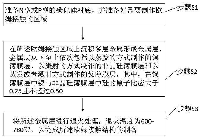
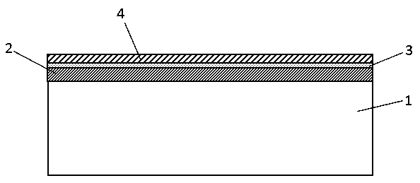
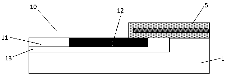
[0036] What the present invention discloses is a kind of preparation method of low-temperature silicon carbide ohmic contact, such as figure 1 As shown, the following steps are included: Step S1: Prepare an N-type or P-type silicon carbide substrate, and form a region 10 where an ohmic contact needs to be made. This region may be the back side of the silicon carbide substrate, or the front N-type epitaxial or P-type epitaxial region, or the front N-type implantation or P-type implantation region. ...


PUM

PropertyMeasurementUnit
thicknessaaaaaaaaaa
thicknessaaaaaaaaaa
thicknessaaaaaaaaaa

Abstract

The invention discloses a method for manufacturing a low-temperature silicon carbide ohmic contact, comprising the following steps of S1, preparing an N-type or P-type silicon carbide substrate, and preparing a region where an ohmic contact is required to be manufactured; S2, depositing layers of metal on the ohmic contact region to form a metal layer, wherein the metal layer includes, in order from bottom to top, a nickel thin film layer formed by evaporation, an amorphous silicon thin film layer formed by sputtering, and a titanium thin film layer formed by evaporation or sputtering, and wherein an atomic ratio of silicon in the nickel thin film layer to nickel in the amorphous silicon thin film layer is greater than 0.25 but less than or equal to 0.50; and S3, annealing the metal layerat an annealing temperature of 600 to 780 degrees centigrade to prepare the ohmic contact structure. The method not only reduces the ohmic contact annealing temperature, but also prevents carbon deposition.

Description

technical field [0001] The invention relates to the field of semiconductor device manufacturing, in particular to a method for preparing a low-temperature silicon carbide ohmic contact and a metal structure. Background technique [0002] As a wide bandgap semiconductor material, silicon carbide (SiC) has attracted more and more attention due to its advantages such as high critical breakdown field strength, low on-resistance, high electron mobility and high thermal conductivity, especially in the power device market, and the application of SiC devices The prospects are very bright. [0003] In the manufacturing process of SiC power devices, the fabrication of electrodes is different from the traditional silicon process due to the high metal-semiconductor barrier, pinning effect, and complex surface states. It has always been the focus and difficulty of the SiC process. For the production of N-type silicon carbide ohmic contacts, it has become common knowledge in the industry...

Claims


Application Information

Patent Timeline
Patent Type & Authority Applications(China)
IPC IPC(8): H01L21/28H01L21/285H01L29/45
CPCH01L21/0485H01L29/45
Inventor 蔡文必陶永洪杨程
Owner HUNAN SANAN SEMICON CO LTD
Why Eureka
Try Eureka