
A kind of encapsulation thin film and its preparation method, optoelectronic device

A technology for encapsulating film and device surface

Active Publication Date: 2021-02-19
TCL CORPORATION
View PDF5 Cites 0 Cited by
  • Summary
  • Abstract
  • Description
  • Claims
  • Application Information

AI Technical Summary

Problems solved by technology

[0006] In view of the above-mentioned deficiencies in the prior art, the purpose of the present invention is to provide a packaging film and its preparation method, and a photoelectric device, aiming to solve the problems of poor water and oxygen barrier performance and thermal conductivity of the existing packaging film

Method used

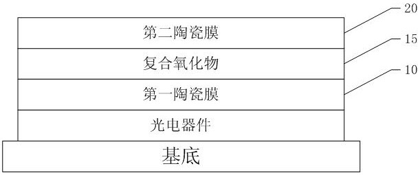

Image

  • A kind of encapsulation thin film and its preparation method, optoelectronic device
  • A kind of encapsulation thin film and its preparation method, optoelectronic device

Examples


preparation example Construction

[0037] Further, the present invention also provides a method for preparing an encapsulation film, wherein, such as figure 2 shown, including steps:

[0038] S1. Provide a device to be packaged, and deposit a first ceramic film on the surface of the device under a reducing atmosphere condition, and the first ceramic film is composed of nitride;

[0039] S2. Depositing a second ceramic film on the surface of the first ceramic film, where the second ceramic film is composed of metal oxide.

[0040] In one embodiment, the first ceramic film is prepared on the surface of the device by magnetron sputtering, and a certain amount of reducing atmosphere is introduced during the process of preparing the first ceramic film, and the reducing atmosphere is hydrogen or carbon dioxide.

[0041] Preferably, the flow rate of the reducing atmosphere is 5-10 sccm.

[0042] Preferably, during the preparation of the first ceramic film, the sputtering power is 50-80W; and / or the sputtering pres...

Embodiment 1

[0051] 1. The structure of the optoelectronic device is: ITO substrate / PEDOT:PSS (50 nm) / poly-TPD (30 nm) / quantum dot light-emitting layer (20 nm) / ZnO (30nm) / silver (70 nm) / encapsulation layer (550nm). Wherein, the material of the packaging film is AlN film / Y 2 o 3 film, the thickness of the AlN film is 500 nm, Y 2 o 3 The film thickness is 50 nm, and both are prepared by RF radio frequency sputtering method.

[0052] 2. The packaging method of the optoelectronic device comprises steps:

[0053] 1) On the top surface of the QLED silver electrode, the AlN target is sputtered into a film by radio frequency sputtering. The sputtering process is: power 60 W, sputtering pressure 0.6 Pa, argon gas flow rate 50 sccm, hydrogen gas The flow rate is 5 sccm, the sputtering time is 25min, and the thickness is about 500 nm;

[0054] 2), the method of radio frequency sputtering is also used to prepare Y 2 o 3 Thin film, the sputtering process is as follows: power 40 W, sputtering pr...

Embodiment 2

[0056] 1. The structure of the optoelectronic device is ITO substrate / PEDOT:PSS (50 nm) / poly-TPD (30 nm) / quantum dot light-emitting layer (20 nm) / ZnO (30nm) / silver (70 nm) / encapsulation layer ( 1100nm). Wherein, the material of the packaging film is AlN film / MgO film, the thickness of the AlN film is 1000 nm, and the thickness of the MgO film is 100 nm, both of which are prepared by RF radio frequency sputtering method.

[0057] 2. The packaging method of the optoelectronic device comprises steps:

[0058] 1) On the top surface of the silver electrode of the QLED, the AlN target is sputtered into a film by radio frequency sputtering. The sputtering process is: power 80 W, sputtering pressure 0.8 Pa, argon gas flow rate 50 sccm, hydrogen gas The flow rate is 5 sccm, the sputtering time is 50min, and the thickness is about 1000 nm;

[0059] 2) The MgO film was also prepared by RF sputtering. The sputtering process was as follows: power 40 W, sputtering pressure 0.5 Pa, argon f...


PUM

PropertyMeasurementUnit
thicknessaaaaaaaaaa
thicknessaaaaaaaaaa
thicknessaaaaaaaaaa

Abstract

The present invention discloses a package thin film and a preparation method thereof, and a photoelectric device. The package thin film comprise a first ceramic film formed by a nitride with a chemical formula of XaNd and a second ceramic film formed by a metallic oxide with a chemical formula of YbOe which are stacked, a composite oxide with a chemical formula of XaYbOc is arranged at the interface between the first ceramic film and the second ceramic film, wherein 1<=a<=3, 1<=b<=3, 2<=c<=6, 1<=d<=4, and 1<=e<=4. In the preparation of the first ceramic film, a reducing atmosphere is introduced, and the surface of the first ceramic film is coated with a layer of the second ceramic film formed by the metallic oxide to effectively reduce the oxygen impurities at the internal portion and thesurface of the first ceramic film so as to allow the package thin film to have good water oxygen blocking effect and thermal conductivity.

Description

technical field [0001] The invention relates to the field of optoelectronic devices, in particular to an encapsulating film, a preparation method thereof, and an optoelectronic device. Background technique [0002] The short life of optoelectronic devices is mainly due to the adsorption of oxygen and water vapor in the air, and the penetration of water vapor in the environment into the device will accelerate the aging of the device, thereby reducing the service life of the device. The organic film and metal electrodes are protected by the packaging process from the influence of external oxygen and water vapor, and finally the purpose of prolonging the life of the device can be achieved, so the packaging process has a great impact on the life of the device. [0003] Traditional optoelectronic device packaging technology is done in a glove box with moisture and oxygen content below 1ppm. The finished device is passed into the glove box by the linear manipulator in the glove b...

Claims


Application Information

Patent Timeline
Patent Type & Authority Patents(China)
IPC IPC(8): H01L33/56
CPCH01L33/56
Inventor 朱佩曹蔚然
Owner TCL CORPORATION
Learn More