Manufacturing method of array substrate, array substrate and display device

The technology of an array substrate and a manufacturing method, which is applied in the field of array substrates and display devices, can solve problems such as uneven light emission of light-emitting diode display devices

Active Publication Date: 2019-07-09
BOE TECH GRP CO LTD +1
View PDF3 Cites 5 Cited by
  • Summary
  • Abstract
  • Description
  • Claims
  • Application Information

AI Technical Summary

Problems solved by technology

[0004] Embodiments of the present invention provide a method for manufacturing an array substrate, an array substrate, and a display device, so as to solve the problem of uneven light emission of an electroluminescent diode display device and alternate light and dark mura at different positions

Method used


Image

  • Manufacturing method of array substrate, array substrate and display device
  • Manufacturing method of array substrate, array substrate and display device
  • Manufacturing method of array substrate, array substrate and display device

Examples


Embodiment Construction

[0019] The following will clearly and completely describe the technical solutions in the embodiments of the present invention with reference to the accompanying drawings in the embodiments of the present invention. Obviously, the described embodiments are some of the embodiments of the present invention, but not all of them. Based on the embodiments of the present invention, all other embodiments obtained by persons of ordinary skill in the art without creative efforts fall within the protection scope of the present invention.

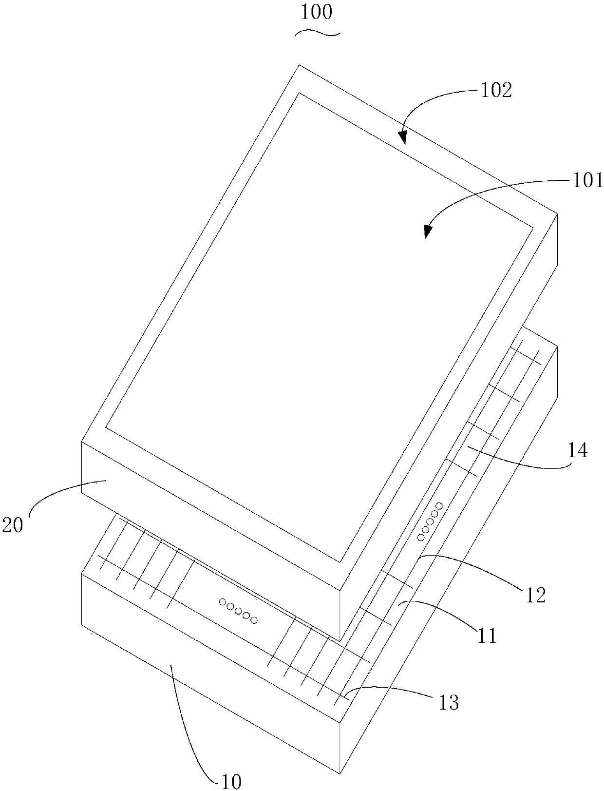
[0020] see figure 1 , figure 1 A perspective view of a display device provided by a preferred embodiment of the present invention. Such as figure 1 As shown, the display device 100 includes an array substrate 10 and an opposite substrate 20, and the array substrate 10 and the opposite substrate 20 are arranged opposite to each other to form a display panel of the display device 100, thereby realizing the display The display function of the device 10...


PUM


Abstract

Embodiments of the invention provide a manufacturing method of an array substrate, the array substrate and a display device. The manufacturing method is characterized by firstly opening a hole on a first thin film transistor, then simultaneously performing hydrogen supplement processing for the first thin film transistor and a second thin film transistor, and opening a hole on the second thin filmtransistor, so that the first thin film transistor and the second thin film transistor can be repaired and compensated to different degrees through the hydrogen supplement processing respectively, wherein, because the hole is opened on the first thin film transistor firstly, the hydrogen supplementing effect of the first thin film transistor is weakened, in this way, the gradient of a current-voltage curve of the first thin film transistor can be properly reduced, a current difference caused by a threshold voltage difference is reduced, and electron mobility of the second thin film transistoris increased as much as possible, the charging electric quantity of a capacitor within the rated time is increased, the current difference between circuits is reduced, therefore, the display device can emit light uniformly, the occurrence probability of Mura is reduced, and the Mura effect is reduced.

Description

technical field [0001] The present invention relates to the field of display technology, in particular to a method for manufacturing an array substrate, the array substrate and a display device. Background technique [0002] Due to the rise of the global information society and the development of science and technology, the field of display technology is changing with each passing day, and there are more and more types of display technologies, such as traditional liquid crystal display technology, organic light-emitting diode (Organic Light-Emitting Diode, OLED) display technology , electrophoretic display technology, etc. Compared with other displays, the organic electroluminescent diode display has the advantages of self-luminous display, fast response speed, high brightness, wide viewing angle, etc., so that it has a wide application prospect. [0003] Although the organic electroluminescent diode display technology has the above-mentioned many advantages, in the existin...

Claims


Application Information

Patent Timeline
Patent Type & Authority Applications(China)
IPC IPC(8): H01L27/32
CPCH10K59/123H10K59/12H01L27/127H01L27/1248H01L27/1222H10K59/1213H10K71/00
Inventor 张陶然曲加伟李林宣廖文骏莫再隆
Owner BOE TECH GRP CO LTD
Why Eureka
Try Eureka