Silicon carbide junction barrier schottky diode and preparation method thereof

A junction barrier Schottky and diode technology, which is applied in semiconductor/solid-state device manufacturing, semiconductor devices, electrical components, etc., can solve the problems of weak interface protection and device breakdown, so as to protect the interface between them and improve breakdown The effect of breakdown voltage and deepening depth

Inactive Publication Date: 2019-07-09
HUAZHONG UNIV OF SCI & TECH
View PDF6 Cites 1 Cited by
  • Summary
  • Abstract
  • Description
  • Claims
  • Application Information

AI Technical Summary

Problems solved by technology

[0006] Aiming at the defects of the prior art, the object of the present invention is to provide a silicon carbide junction barrier Schottky diode and its preparation method, aiming to solve the problems of the existing silicon carbide junction barrier Schottky diode due to the shallow depth of the field limiting ring. , so that the position of the peak electric field is close to the interface between the drift layer and the passivation layer, and the protection effect on the interface is weak, leading to the problem of early breakdown of the device

Method used


Image

  • Silicon carbide junction barrier schottky diode and preparation method thereof
  • Silicon carbide junction barrier schottky diode and preparation method thereof
  • Silicon carbide junction barrier schottky diode and preparation method thereof

Examples


Embodiment Construction

[0043] In order to make the object, technical solution and advantages of the present invention clearer, the present invention will be further described in detail below in conjunction with the accompanying drawings and embodiments. It should be understood that the specific embodiments described here are only used to explain the present invention, not to limit the present invention.

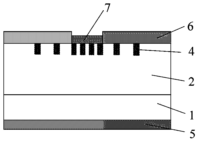
[0044] The SiC junction barrier Schottky diode structure with traditional field limiting ring termination is shown as figure 1 As shown, due to the limitation of the ion implantation process, the depth of the field limiting ring 4 is less than 1 μm, and in silicon carbide devices, the peak position of the electric field is usually at the lower boundary of the field limiting ring, and the shallower implantation depth makes the position of the peak electric field close to the drift The interface between the layer 2 and the passivation layer 6 has a weak protective effect on the interface, and the eff...


PUM


Abstract

The invention discloses a silicon carbide junction barrier schottky diode and a preparation method thereof. The silicon carbide junction barrier schottky diode comprises a cathode electrode, a siliconcarbide substrate, a first drift layer and a second drift layer which are arranged in turn from the bottom to the top and first field limiting rings, second field limiting rings, a passivation layerand an anode electrode. The depth of the first field limiting rings is less than that of the first drift layer and the first field limiting rings are distributed in the first drift layer in a spaced way and leveled with the upper surface of the first drift layer. The width of the second field limiting rings is less than that of the first field limiting rings and the depth is the same as that of the second drift layer and the second field limiting rings are distributed in the second drift layer in a spaced way. The first field limiting rings and the second field limiting rings are identical innumber and correspondingly in the inverted T-shape or n L-shape distribution. The anode electrode is located on the main junction, and the passivation layer is located on both sides of the anode electrode. The breakdown voltage of the schottky diode is increased and the difficulty of the preparation process is reduced.

Description

technical field [0001] The invention belongs to the technical field of semiconductor devices, and more specifically relates to a silicon carbide junction barrier Schottky diode and a preparation method thereof. Background technique [0002] Since silicon carbide has a wider band gap, higher thermal conductivity, higher electron saturation rate and higher critical breakdown electric field than silicon, the devices made of it can withstand harsh conditions such as high temperature and high pressure. , make up for the shortage of traditional silicon materials, and have broad application prospects in power devices. [0003] As the earliest commercialized diode, silicon carbide Schottky diode is not affected by the charge storage effect, has fast switching speed and low on-resistance, but is significantly affected by the barrier lowering effect under high voltage conditions, which limits Its application in the high-voltage field; compared with the Schottky diode, the PiN diode h...

Claims


Application Information

Patent Timeline
Patent Type & Authority Applications(China)
IPC IPC(8): H01L29/06H01L21/336H01L29/872
CPCH01L29/0619H01L29/6606H01L29/872
Inventor 吴燕庆胡奔李学飞
Owner HUAZHONG UNIV OF SCI & TECH
Why Eureka
Try Eureka