Cavity type bulk acoustic wave resonator with stress buffer layer and preparation method thereof

A technology of bulk acoustic wave resonator and stress buffer layer, which is applied to electrical components, impedance networks, etc., can solve problems affecting device quality, thermal stress mismatch, and silicon substrate without stress buffering effect, so as to improve the preparation quality and avoid The effect of film cracking

Active Publication Date: 2019-07-12
UNIV OF ELECTRONICS SCI & TECH OF CHINA
View PDF10 Cites 9 Cited by
  • Summary
  • Abstract
  • Description
  • Claims
  • Application Information

AI Technical Summary

Problems solved by technology

[0004] Usually, the main structure of the thin film bulk acoustic resonator is bonded on the silicon substrate. Since the thermal expansion coefficients of the silicon substrate, the bonding layer, and the piezoelectric film layer are not uniform, and the traditional silicon substrate has no stress buffering effect, The piezoelectric film is prepared by the wafer bonding transfer process, which will cause thermal stress mismatch between the piezoelectric film layer and the substrate, the piezoelectric film layer and the bonding layer, and the bonding layer and the substrate, resulting in piezoelectric film Warpage and cracks occur, seriously affecting the quality of the device

Method used


Image

  • Cavity type bulk acoustic wave resonator with stress buffer layer and preparation method thereof
  • Cavity type bulk acoustic wave resonator with stress buffer layer and preparation method thereof
  • Cavity type bulk acoustic wave resonator with stress buffer layer and preparation method thereof

Examples


Embodiment 1

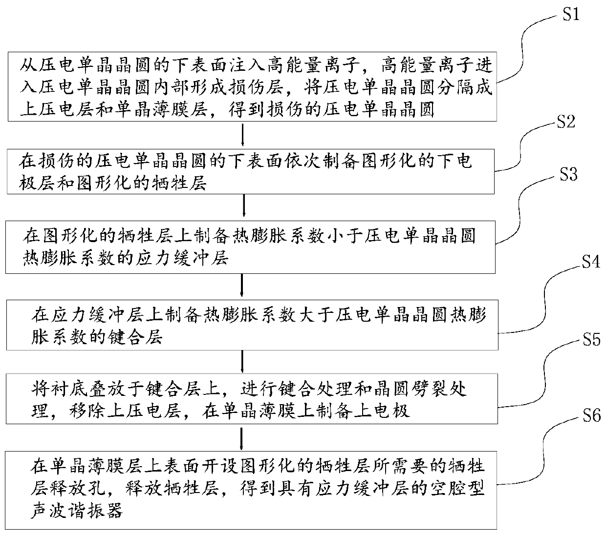
[0066] Such as figure 1 , figure 2 , image 3 , Figure 4 , Figure 5 , Image 6 , Figure 7 , Figure 8 , Figure 9 As shown, a method for preparing a cavity-type bulk acoustic resonator with a stress buffer layer includes the following steps: the piezoelectric single crystal wafer selected in this embodiment is a lithium niobate piezoelectric single crystal wafer;

[0067] S1) High-energy ions A are implanted from the lower surface of the lithium niobate piezoelectric single crystal wafer, and the high-energy ions A enter the piezoelectric single crystal wafer to form a damaged layer 8, which separates the piezoelectric single crystal wafer into upper piezoelectric single crystal wafers. Layer 9 and single crystal thin film layer 1 to obtain a damaged piezoelectric single crystal wafer; preferably, high-energy ions include hydrogen ions (preferably positive monovalent hydrogen ions, H + ), helium ions (preferably positive monovalent helium ions, He + ), boron ion (...

Embodiment 2

[0089] Such as Figure 10 As shown, a method for preparing a cavity-type bulk acoustic resonator with a stress buffer layer in this embodiment includes the following steps: the piezoelectric single crystal wafer selected in this embodiment is lithium niobate piezoelectric single crystal round;

[0090] S11) Implanting high-energy ions from the lower surface of the lithium niobate piezoelectric single-crystal wafer, the high-energy ions enter the interior of the piezoelectric single-crystal wafer to form a damaged layer, and separate the piezoelectric single-crystal wafer into an upper piezoelectric layer and a single piezoelectric layer. crystal thin film layer to obtain damaged piezoelectric single crystal wafers; high-energy ions include hydrogen ions (preferably positive monovalent hydrogen ions, H + ), helium ions (preferably positive monovalent helium ions, He + ), boron ion (preferably positive monovalent boron ion, B + ) or arsenic ions (preferably positive monovalen...

Embodiment 3

[0109] Such as Figure 11 As shown, a method for preparing a cavity-type bulk acoustic resonator with a stress buffer layer in this embodiment includes the following steps: the piezoelectric single crystal wafer selected in this embodiment is lithium niobate piezoelectric single crystal round;

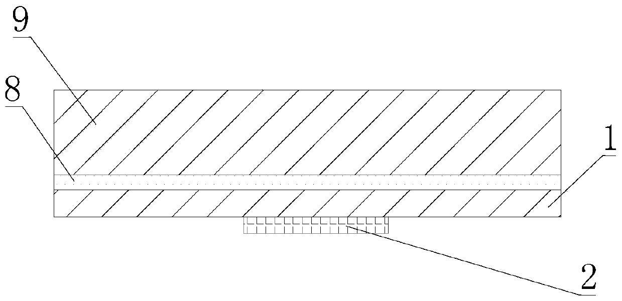
[0110] S21) Implanting high-energy ions from the lower surface of the lithium niobate piezoelectric single-crystal wafer, the high-energy ions enter the interior of the piezoelectric single-crystal wafer to form a damaged layer, and separate the piezoelectric single-crystal wafer into an upper piezoelectric layer 9 and Single crystal thin film layer 1, obtains the damaged piezoelectric single crystal wafer; High-energy ions include hydrogen ions (preferably positive monovalent hydrogen ions, H + ), helium ions (preferably positive monovalent helium ions, He + ), boron ion (preferably positive monovalent boron ion, B + ) or arsenic ions (preferably positive monovalent arsenic ions, A...


PUM


Abstract

The invention relates to the technical field of bulk acoustic wave resonator preparation, in particular to a cavity type bulk acoustic wave resonator with a stress buffer layer and a preparation method of the cavity type bulk acoustic wave resonator. The method comprises the following steps: preparing a lower electrode and a graphical sacrificial layer on a piezoelectric single crystal wafer witha damage layer; preparing a stress buffer layer on the graphical sacrificial layer; preparing a bonding layer on the stress buffer layer; stacking the substrate on the bonding layer, performing bonding processing and wafer splitting processing, removing the upper piezoelectric layer, and preparing an upper electrode; forming a sacrificial layer release hole required by the graphical sacrificial layer on the upper surface of the single crystal film layer, and releasing the sacrificial layer to obtain the cavity type bulk acoustic wave resonator with the stress buffer layer; through the design that the stress buffer layer is arranged between the single crystal thin film layer and the bonding layer, the problems that in the existing bonding process, the single crystal thin film cracks, tilts,sinks, even falls off and the like due to too large interface stress are solved, and the performance of the cavity type bulk acoustic wave resonator is improved.

Description

technical field [0001] The invention relates to the technical field of bulk acoustic wave resonator preparation, in particular to a cavity-type bulk acoustic wave resonator with a stress buffer layer and a preparation method thereof. Background technique [0002] At present, the structures of thin film bulk acoustic resonators mainly include solid assembly type (SMR) and cavity type, and the cavity type thin film bulk acoustic resonator is simpler than the solid assembly type. The working principle of the film bulk acoustic resonator is to use the impedance mismatch of the interface between the electrode and the air to limit the sound wave between the upper and lower electrodes to achieve resonance. The resonator with this structure has a high quality factor (Q value), often greater than 1000, low insertion loss, and compatibility with complementary metal oxide semiconductor (CMOS) circuits. [0003] The piezoelectric film of the existing thin film bulk acoustic resonator i...

Claims


Application Information

Patent Timeline
Patent Type & Authority Applications(China)
IPC IPC(8): H03H3/02H03H9/17H03H9/02
CPCH03H3/02H03H9/171H03H9/02102H03H9/02133H03H2003/023
Inventor 罗文博帅垚吴传贵
Owner UNIV OF ELECTRONICS SCI & TECH OF CHINA
Why Eureka
Try Eureka