
III-nitride enhanced HEMT based on composite barrier layer structure and manufacturing method of III-nitride enhanced HEMT

A technology of compound potential barrier and fabrication method, applied in III-nitride enhanced HEMT and fabrication thereof, field effect transistor device field, can solve the problem of inability to meet device reliability requirements, lower gate threshold voltage swing, and forward gate The problems such as the increase of electrode leakage can achieve the effect of ensuring on-chip uniformity, improving gate threshold voltage swing, and suppressing forward gate leakage.

Active Publication Date: 2019-07-19
SUZHOU INST OF NANO TECH & NANO BIONICS CHINESE ACEDEMY OF SCI
View PDF5 Cites 12 Cited by
  • Summary
  • Abstract
  • Description
  • Claims
  • Application Information

AI Technical Summary

Problems solved by technology

However, since the gate region still adopts a low Al composition and a thin barrier layer structure, the potential barriers for p-type layer holes and channel layer electrons are relatively low, so it is very easy to cause the device to leak to the gate. increase, the gate threshold voltage swing becomes lower, which cannot meet the reliability requirements of the actual operation of the device, and the electrochemical corrosion and slow etching technology are used in the preparation process of the groove gate, so the process is complicated and difficult to control, which is not conducive to mass production

Method used


Image

  • III-nitride enhanced HEMT based on composite barrier layer structure and manufacturing method of III-nitride enhanced HEMT
  • III-nitride enhanced HEMT based on composite barrier layer structure and manufacturing method of III-nitride enhanced HEMT
  • III-nitride enhanced HEMT based on composite barrier layer structure and manufacturing method of III-nitride enhanced HEMT

Examples


Embodiment 1

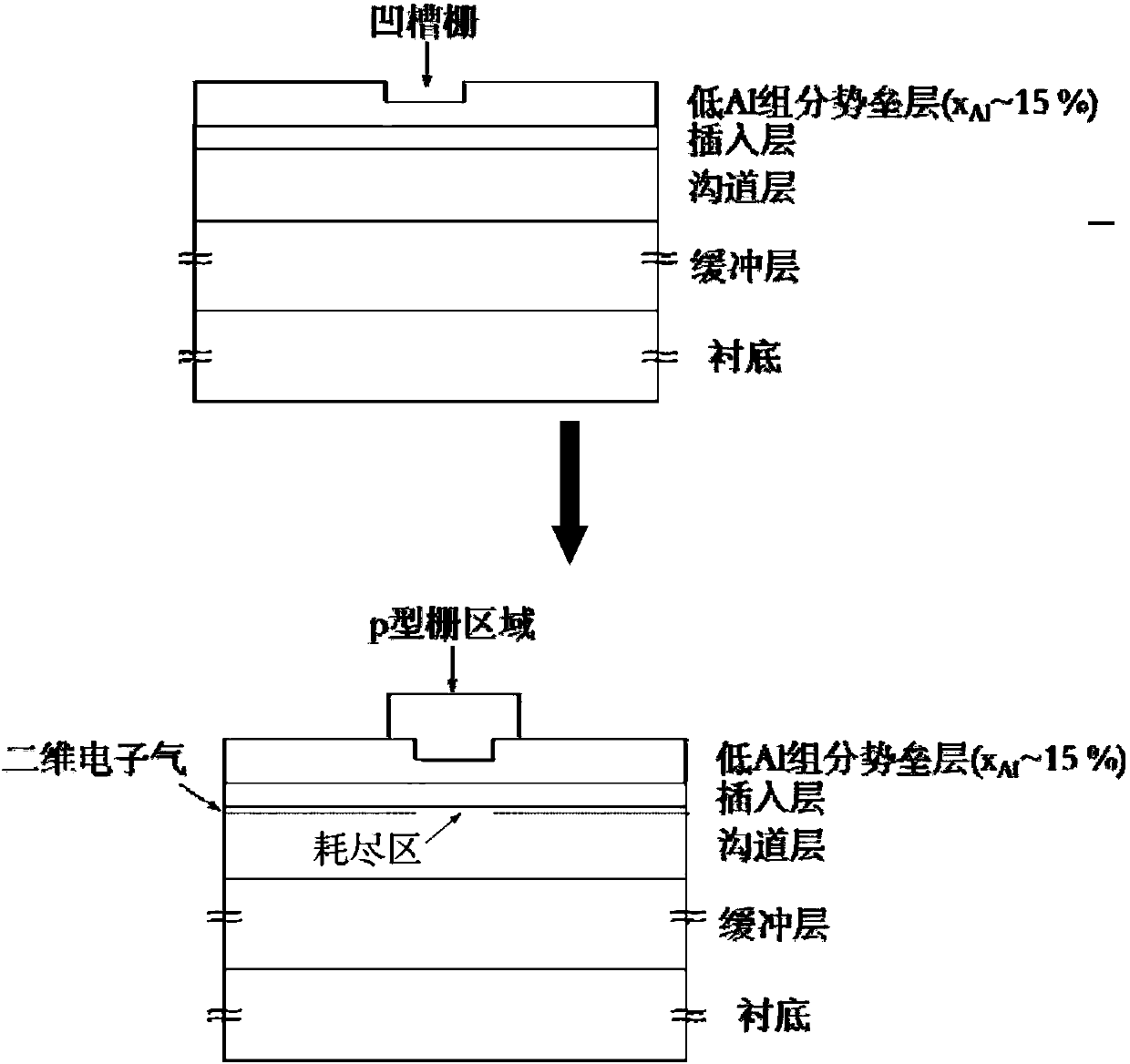
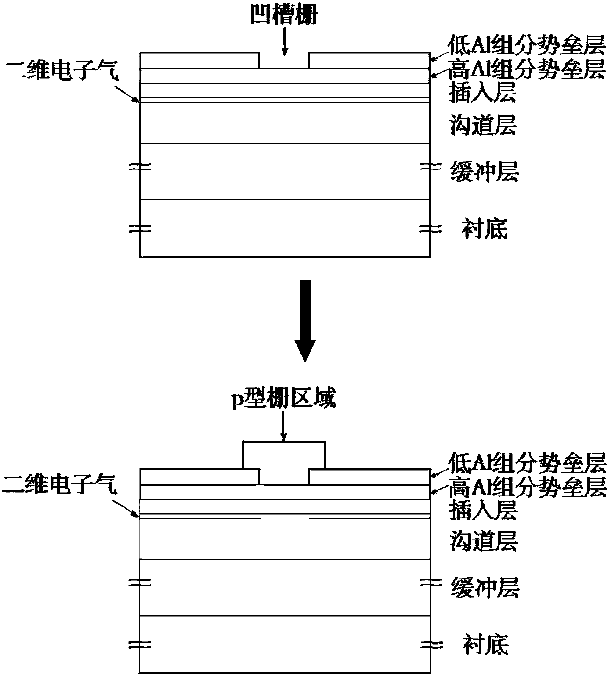
[0095] Embodiment 1 A kind of based on Al 0.15 Ga 0.85 N / Al 0.30 Ga 0.70 The fabrication method of the HEMT of the N double potential barrier layer comprises the following steps:

[0096] Step S1: MOCVD epitaxial growth of HEMT based on AlGaN double barrier layer heterojunction. The upper barrier layer is an AlGaN barrier layer with a low Al composition, the Al composition is 15%, and the thickness is 20-35nm; the lower barrier layer is a high Al composition AlGaN barrier layer, the Al composition is 30%, and the thickness is 20-35nm. 5-10nm. The AlN insertion layer is about 1nm; the GaN channel layer is 50-200nm. HEMT epitaxial structures such as Figure 4 shown. The buffer layer can be made of GaN or AlGaN with graded Al composition, or a combination of both; the substrate can be made of sapphire, silicon carbide, gallium nitride or aluminum nitride.

[0097] Step S2: Groove gate etching. The photoresist AZ5214 is used as a mask, and the groove gate is etched by ICP...

Embodiment 2

[0104] Embodiment 2 A kind of based on Al 0.15 Ga 0.85 N / AlN / Al 0.30 Ga 0.70 The manufacturing method of the HEMT of N multi-barrier layer comprises the following steps:

[0105] Step S1: MOCVD epitaxial growth of HEMT based on AlGaN multi-barrier layer heterojunction, that is, a sandwich-type AlGaN barrier layer structure containing AlN insertion layer: the upper barrier layer is an AlGaN barrier layer with a low Al composition, and the Al composition The lower barrier layer is an AlGaN barrier layer with a high Al composition, the Al composition is 30%, and the thickness is 5-10nm; between the two is a thin AlN layer with a thickness of about 1-30nm. 2nm, the role of this layer is to provide a wider process window for self-terminating etching, making the trench gate etching process more stable and reliable. In addition, the AlN insertion layer is about 1nm; the GaN channel layer is 50-200nm. HEMT epitaxial structures such as Figure 13 shown. Wherein, the buffer layer...


PUM


Abstract

The invention discloses a III-nitride enhanced HEMT based on a composite barrier layer structure and a manufacturing method of the III-nitride enhanced HEMT. The HEMT comprises a first semiconductor,a second semiconductor, a third semiconductor serving as a p-type layer, a source electrode, a drain electrode, a grid electrode and the like, wherein the first semiconductor and the second semiconductor respectively serve as a channel layer and a barrier layer, a groove structure is formed in the area, corresponding to the grid electrode, of the barrier layer, the groove structure cooperates withthe third semiconductor and the grid electrode to form a p-type grid, and the second semiconductor comprises a first structure layer and a second structure layer which are sequentially arranged on the first semiconductor. Compared with a mode of determining an etching reagent, the first structure layer has higher etching resistance than the second structure layer. The HEMT structure can be more accurately regulated and controlled, meanwhile, the HEMT has the better device performance. For example, the forward gate leakage and gate threshold voltage swing amplitude are remarkably improved, thein-chip uniformity of threshold voltage of the device can be guaranteed, and meanwhile, the HEMT structure is easier to manufacture and suitable for large-scale production.

Description

technical field [0001] The invention relates to a field effect transistor device, in particular to a III-nitride-enhanced HEMT based on a compound barrier layer structure and a manufacturing method thereof, belonging to the field of semiconductor technology. Background technique [0002] Compared with traditional silicon-based MOSFETs, high electron mobility transistors (High Electron Mobility Transistors, HEMTs) based on heterojunctions such as AGaN / AlN / GaN have unique advantages such as low on-resistance, high breakdown voltage, and high switching frequency. , so that it can be used as a core device in various power conversion systems, and has important application prospects in energy saving and consumption reduction, so it has received great attention from academia and industry. However, due to the polarization effect of the III-nitride material system, generally speaking, HEMTs based on AlGaN / AlN / GaN heterojunctions are depletion mode (normally on). When this type of dev...

Claims


Application Information

Patent Timeline
Patent Type & Authority Applications(China)
IPC IPC(8): H01L29/778H01L21/335
CPCH01L29/7786H01L29/66462H01L29/1066H01L29/205H01L29/41766H01L29/2003H01L29/475H01L29/7783
Inventor 孙钱周宇钟耀宗高宏伟冯美鑫杨辉
Owner SUZHOU INST OF NANO TECH & NANO BIONICS CHINESE ACEDEMY OF SCI
Learn More