Heterojunction back-contact solar cell and fabrication method thereof
A solar cell and back contact technology, applied in circuits, electrical components, photovoltaic power generation, etc., can solve problems affecting battery conversion efficiency, increase in series resistance, light absorption loss, etc.
- Summary
- Abstract
- Description
- Claims
- Application Information
AI Technical Summary
Problems solved by technology
Method used
Image
Examples
Embodiment
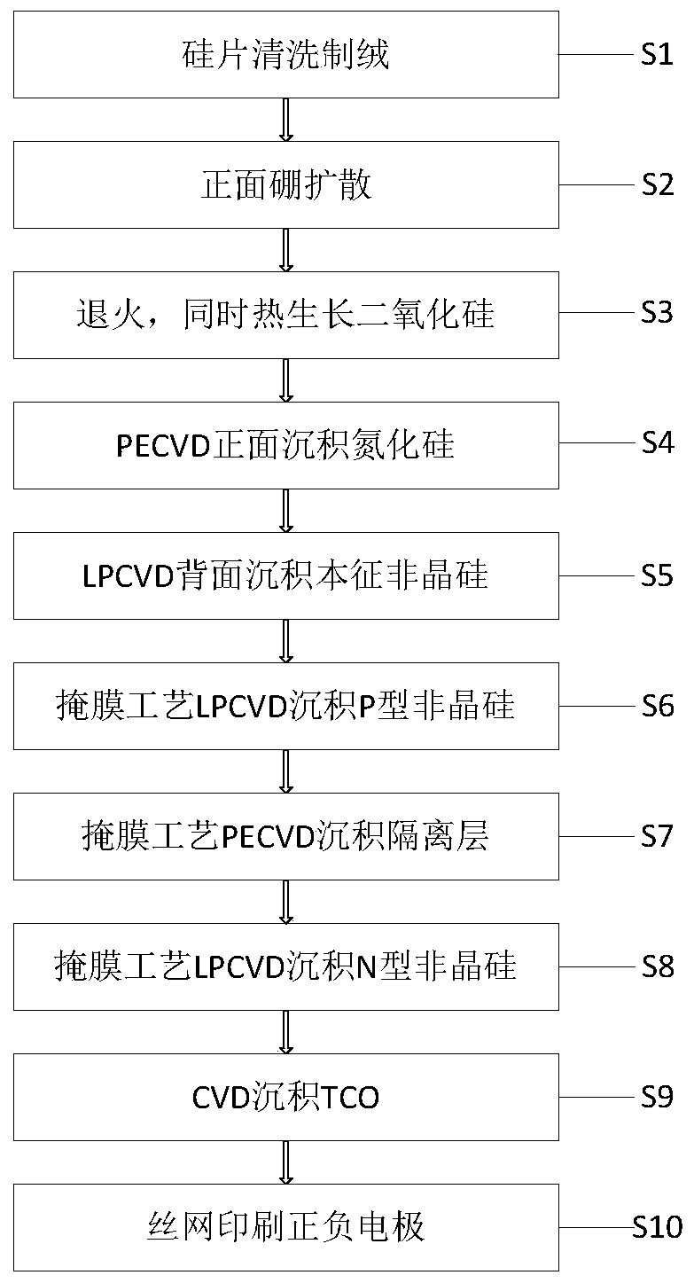
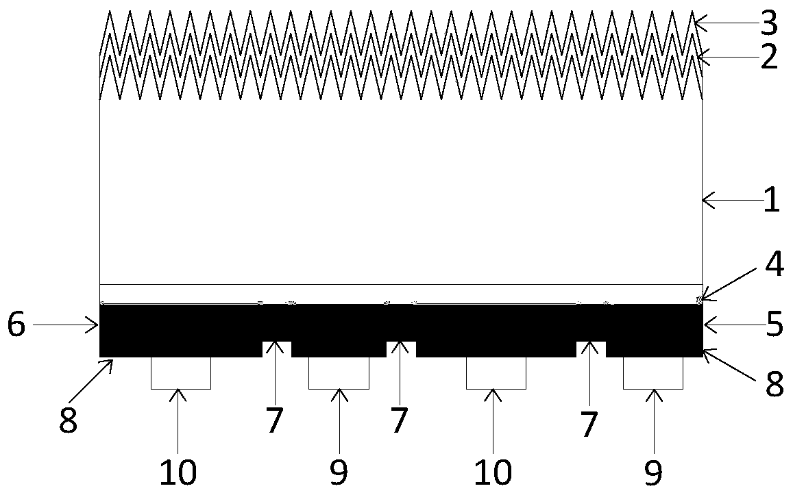
[0036] like figure 1 As shown, the heterojunction back-contact solar cell of the present invention includes an N-type monocrystalline silicon substrate 1, and a front surface P+ doped layer 2 and an anti-reflection layer 3 are sequentially arranged on the front of the N-type monocrystalline silicon substrate 1. An intrinsic amorphous silicon layer 4 is arranged on the back of the N-type monocrystalline silicon substrate 1, and an N-type amorphous silicon doped layer 5 and a P-type amorphous silicon doped layer 6 are respectively arranged on the back of the intrinsic amorphous silicon layer 4. , an insulating isolation layer 7 is arranged between the N-type amorphous silicon doped layer 5 and the P-type amorphous silicon doped layer 6, the N-type amorphous silicon doped layer 5 is connected to a negative electrode 9 through a TCO layer 8, and the P-type The amorphous silicon doped layer 6 is connected to a positive electrode 10 through a TCO layer 8 .
[0037] In this embodime...
PUM
 Abstract
Description
Claims
Application Information
 - R&D
- Intellectual Property
- Life Sciences
- Materials
- Tech Scout
- Unparalleled Data Quality
- Higher Quality Content
- 60% Fewer Hallucinations
Browse by: Latest US Patents, China's latest patents, Technical Efficacy Thesaurus, Application Domain, Technology Topic, Popular Technical Reports.
© 2025 PatSnap. All rights reserved.Legal|Privacy policy|Modern Slavery Act Transparency Statement|Sitemap|About US| Contact US: help@patsnap.com


