
Liquid crystal on silicon (LCOS) chip and LCOS module

A chip and orientation layer technology, applied in nonlinear optics, instruments, optics, etc., can solve the problems of LCOS chips and LCOS modules difficult to apply high-energy laser imaging and modulation, and achieve simplified structure, improved anti-glare resistance, high efficiency The effect of heat dissipation

Pending Publication Date: 2019-07-26
XIAN MICROMACH TECH CO LTD
View PDF0 Cites 0 Cited by
  • Summary
  • Abstract
  • Description
  • Claims
  • Application Information

AI Technical Summary

Problems solved by technology

[0005] The purpose of the present invention is to provide a kind of LCOS chip and LCOS module, aim at solving the technical problem that LCOS chip and LCOS module are difficult to be applied to the imaging and modulation of high-energy laser in the prior art

Method used


Image

  • Liquid crystal on silicon (LCOS) chip and LCOS module
  • Liquid crystal on silicon (LCOS) chip and LCOS module
  • Liquid crystal on silicon (LCOS) chip and LCOS module

Examples


Embodiment 1

[0025] as attached figure 1 As shown, the LCOS chip 10 provided by this embodiment includes a silicon substrate 101, a dielectric film 102, an alignment layer 103, a liquid crystal 104, an alignment layer 103, and an ITO glass 105 from bottom to top, and the silicon substrate 101 and the ITO glass 105 are passed through epoxy Resin glue 106 bonds the package.

[0026] Optionally, the alignment layer 103 may be an organic alignment layer or an inorganic alignment layer.

[0027] Since the light damage threshold of the inorganic alignment layer is higher, it can withstand stronger laser irradiation than the organic alignment layer.

[0028] Specifically, the inorganic alignment layer is a silicon oxide material, and a small-angle silicon oxide thin film is prepared on the ITO glass 105 and the silicon substrate 101 coated with the dielectric film 102 by electron beam evaporation coating method and using an oblique evaporation process. The LCOS chip 10 is used for 810nm wavelen...

Embodiment 2

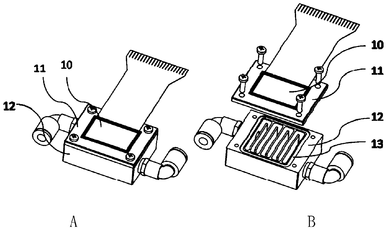
[0034] as attached Figure 2-3 As shown, in the LCOS module shown in the second embodiment, the LCOS module includes the LCOS chip shown in the first embodiment.

[0035] Optionally, in addition to the LCOS chip 10, the LCOS module also includes a water-cooled heat sink 12 and a cover plate 11, the LCOS chip 10 is embedded in the cover plate 11, and the lower surface of the cover plate 11 is attached to the water-cooled heat sink 12.

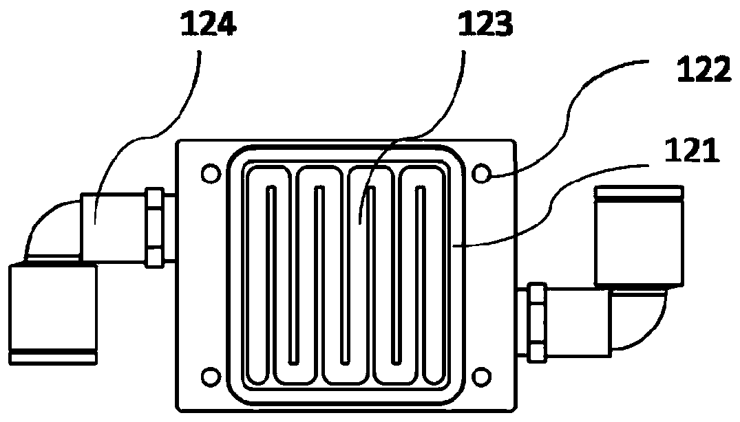
[0036] Please refer to figure 2 , which is a schematic structural diagram of a water-cooled heat sink 12 according to an embodiment of the present invention.

[0037] Such as figure 2 As shown, the water path in the water-cooled heat sink 12 is a "snake-like" microchannel structure 123. In the microchannel structure 123, the two ends of the microchannel are through holes connected to the outside world, and the outer through holes can be connected with the hose transfer valve 124 connect. The edge of the microchannel is a closed-loop groov...


PUM


Abstract

The invention is suitable for the technical field of displayers, and provides a liquid crystal on silicon (LCOS) chip and an LCOS module. According to the LCOS chip, a dielectric film is introduced into the LCOS chip to isolate light from a silicon substrate, the high light resistance of the whole chip is improved, thus the LCOS chip can be applied to imaging and modulation of a high-energy laser,a water-cooling heat sink in the LCOS module adopts the microchannel structure design, thus the contact face of a water flow and the heat sink is increased maximally, and the efficient heat dissipation effect is achieved; and the LCOS chip is designed as a heat sink cover plate, thus the water flow directly makes contact with an LCOS back plate, the design has the more-efficient heat dissipationeffect, and meanwhile, the structure of the LCOS module is simplified.

Description

technical field [0001] The invention belongs to the technical field of displays, and in particular relates to an LCOS chip and an LCOS module. Background technique [0002] LCOS (Liquid Crystal on Silicon, liquid crystal on silicon) is a reflective, very small matrix liquid crystal display device. The LCOS chip usually includes: a silicon substrate, on which MOS transistors are formed; an ITO glass substrate, which is packaged with the silicon substrate; a liquid crystal layer, which is located between the silicon substrate and the glass substrate Between: the alignment layer, the alignment layer is respectively distributed between the liquid crystal layer and the glass substrate, the liquid crystal layer and the silicon substrate, and plays the role of liquid crystal alignment. [0003] The LCOS chip uses metal material as the pixel electrode and forms an image through the principle of light reflection, so it is called a reflective liquid crystal microchip. LCOS can modul...

Claims


Application Information

Patent Timeline
IPC IPC(8): G02F1/13G02F1/1333
CPCG02F1/1313G02F1/1333G02F1/133382
Inventor 高峰王海波王华杨小君
Owner XIAN MICROMACH TECH CO LTD
Learn More