

Organic light-emitting device
A technology of organic light-emitting devices and dimming areas, which is applied in the direction of electric solid-state devices, semiconductor devices, electrical components, etc., can solve the problems of low light-emitting aperture ratio, decreased screen life, and low effective aperture ratio, so as to improve optical dispersion characteristics , improve life and performance, and improve the effect of effective opening ratio
- Summary
- Abstract
- Description
- Claims
- Application Information
AI Technical Summary
Problems solved by technology
Method used
Image

Examples
Embodiment 2
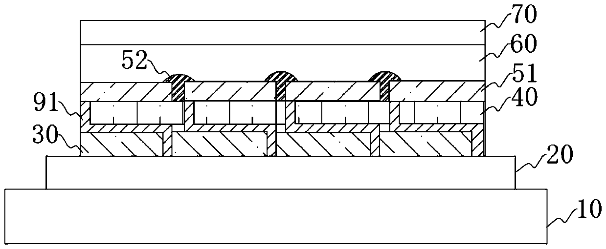
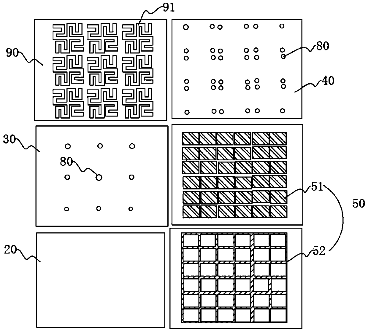
[0063] Such as Figure 4 and Figure 5 As shown, on the basis of Embodiment 1, the anti-short circuit structure layer 90 in this embodiment also includes a number of dimming areas 92 that are not in contact with the circuit protection device 91, that is, the dimming areas 92 and the The circuit protection device 91 is non-conductive; the thickness of the dimming area 92 is not uniform, for example, the dimming area 92 can be hill-shaped, saw-toothed or wave-shaped, etc., and the thickness at the highest point is 200um. In the embodiment, its thickness can also be other values in the range of 20nm to 300um.
[0064] The bottom surface of the dimming area can be, for example, a circle, a square, or other regular or irregular shapes.
[0065] The dimming area can be achieved by patterning design with homogeneous materials with the circuit protection device, for example, both are made of indium tin oxide; it can also be achieved by coating with heterogeneous materials such as ...
Embodiment 3
[0068] On the basis of Embodiment 1, the anti-short circuit structure layer 90 in this embodiment also includes several dimming areas that are not in contact with the circuit protection device 91, that is, the dimming areas are not in contact with the circuit protection device 91. Conductive; the dimming area is composed of transparent resin mixed with high refractive index scattering particles (such as titanium dioxide or zirconia nanometers), or composed of transparent resin mixed with micro lenses to form an optical scattering junction; the maximum thickness of the dimming area 30um, and the insulating area of the second insulating layer evenly covers the dimming area and the circuit protection device, so as to ensure that the dimming area does not have any contact with the pixel 51, and ensure that the circuit protection device is in contact with the pixel 51 except for the part passing through the through hole 80. Except for the contact, other parts are not in contact wi...
PUM
| Property | Measurement | Unit |
|---|---|---|
| Thickness | aaaaa | aaaaa |
| Thickness | aaaaa | aaaaa |
| Resistance | aaaaa | aaaaa |
Abstract
Description
Claims
Application Information