Preparation method of photodiodes, photodiode and CMOS image sensor

A photodiode and lithography technology, applied in the direction of diodes, electric solid-state devices, circuits, etc., can solve problems such as output image quality degradation, white spots, and carrier residues

Active Publication Date: 2019-08-02
SHENZHEN GOODIX TECH CO LTD
View PDF6 Cites 2 Cited by
  • Summary
  • Abstract
  • Description
  • Claims
  • Application Information

AI Technical Summary

Problems solved by technology

However, this method will cause the carrier in the central area of ​​the photodiode to be difficult to deplete, so that there will be carrier residues, making it difficult for the pixel unit to transfer all the carriers when outputting an image, resulting in a decrease in the quality of the output image, such as image smearing , dark current is too large or white spots and other problems

Method used


Image

  • Preparation method of photodiodes, photodiode and CMOS image sensor
  • Preparation method of photodiodes, photodiode and CMOS image sensor
  • Preparation method of photodiodes, photodiode and CMOS image sensor

Examples


preparation example Construction

[0048] Figure 4 Schematic flow chart of the preparation method of the photodiode provided by the application Figure 1 . Figure 4 The execution subject of the shown method flow can be the preparation device of photodiode, such as Figure 4 As shown, the preparation method of the photodiode provided in this embodiment may include:

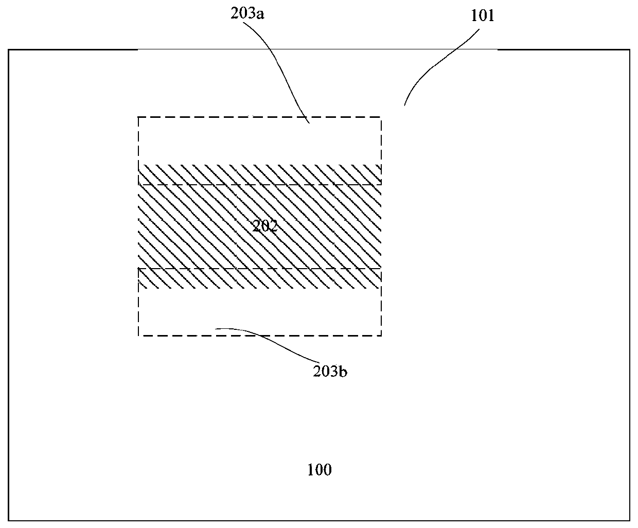
[0049] S401, forming a shielding layer on the substrate, the substrate has a first doping type, and a preset position is set on the substrate, the preset position is a position where the doping type is the second doping type, and the first doping type Different from the second doping type, the shielding layer is used to shield ions implanted into the substrate, and the shielding strength of the shielding layer is related to the thickness of the shielding layer.

[0050] The photodiode preparation device in this embodiment can be a device that integrates multiple functions such as coating, photolithography, etching, and ion implantation, and can...


PUM


Abstract

The invention provides a preparation method of photodiodes, a photodiode and a CMOS image sensor. The preparation method includes: forming a shielding layer on a substrate, wherein the substrate has afirst doping type, and a preset position is arranged on the substrate, and the first doping type and the second doping type are different; processing the shielding layer to enable the thickness of the shielding layer above the preset position to be smaller than the thickness of the shielding layer above the non-preset position; performing ion implantation on the substrate, so that the implanted ions are formed into a curved surface having a second doping type to increase a contact area of the substrate and the region; and removing the shielding layer to obtain a photodiode. The preparation method of photodiodes increases the contact area of the substrate having a first doping type with a region having a second doping type, and increases the full well capacity.

Description

technical field [0001] The present application relates to the technical field of image sensor manufacturing, in particular to a method for preparing a photodiode, a photodiode and a CMOS image sensor. Background technique [0002] Metal complementary oxide semiconductor (CMOS) solid-state image sensor (CMOS Image Sensor) is a sensor that converts incident light signals into electrical signals, and is widely used in smart phones, digital cameras, driving recorders, and security monitoring equipment. A CMOS image sensor is composed of a plurality of pixel units, that is, a pixel array, and each pixel unit corresponds to at least one photodiode. [0003] The working principle of the CMOS image sensor is: when light hits the pixel unit of the image sensor, the photodiode corresponding to the pixel unit generates a corresponding amount of charges according to the incident light intensity, and these charges are transferred to the pixel unit after analog-to-digital conversion and s...

Claims


Application Information

Patent Timeline
Patent Type & Authority Applications(China)
IPC IPC(8): H01L31/18H01L31/0352H01L31/101H01L27/146
CPCH01L31/1804H01L31/101H01L31/0352H01L27/1461H01L27/14643Y02P70/50
Inventor 姚国峰沈健
Owner SHENZHEN GOODIX TECH CO LTD
Why Eureka
Try Eureka