Deep ultraviolet LED epitaxial structure, preparation method thereof, and deep ultraviolet LED
An epitaxial structure, deep ultraviolet technology, applied in the direction of electrical components, circuits, semiconductor devices, etc., can solve the problems of restricting the development of commercialization and low luminous efficiency, and achieve improved hole injection rate, high luminous efficiency, and improved internal quantum efficiency and the effect of transmit power
- Summary
- Abstract
- Description
- Claims
- Application Information
AI Technical Summary
Problems solved by technology
Method used
Image

Examples
Embodiment 1
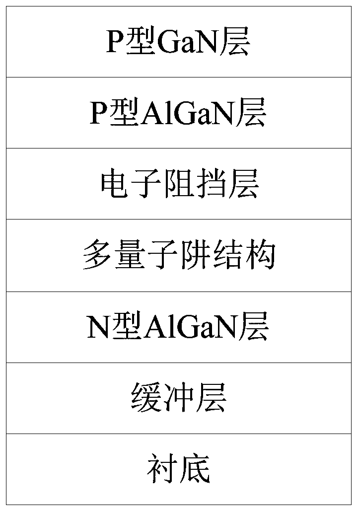
[0054] This embodiment provides a deep ultraviolet LED epitaxial structure, such as figure 1 and figure 2 As shown, it includes a substrate and a buffer layer, an N-type AlGaN layer, a multi-quantum well structure, an electron blocking layer, a P-type AlGaN layer, and a P-type GaN layer that are sequentially stacked upward from the substrate;
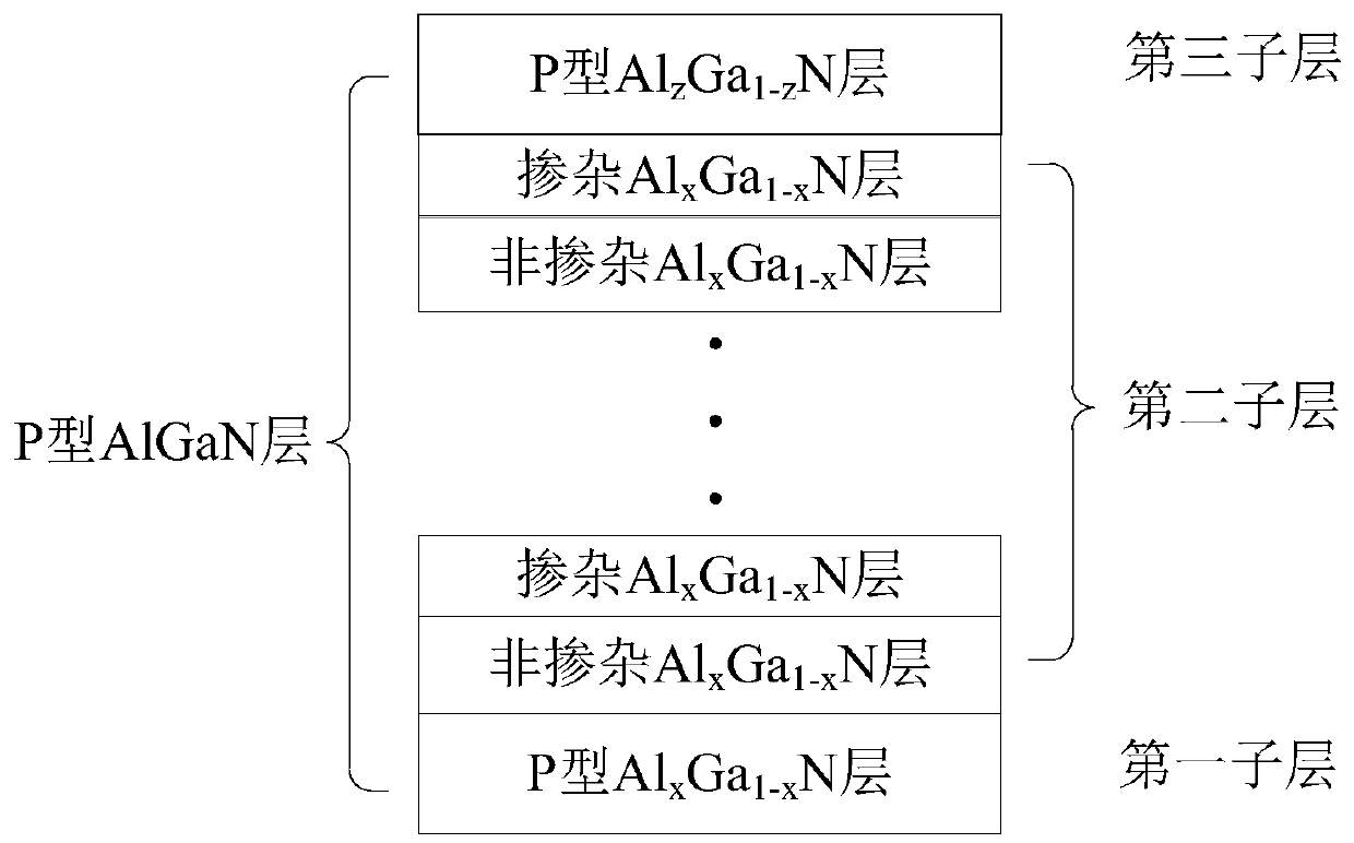
[0055] Wherein, from the substrate upwards, the P-type AlGaN layer includes a first sublayer, a second sublayer and a third sublayer which are sequentially stacked; the first sublayer is P-type Al x Ga 1-x N layer; the second sub-layer includes non-doped Al alternately stacked y Ga 1-y N layer and doped Al y Ga 1-y N layer, alternating times ≥ 1; the third sublayer is P-type Al z Ga 1-z N layers, 1>x>y>z>0.
[0056] The preparation process of the deep ultraviolet LED epitaxial structure is as follows:
[0057] 1. Place the c-plane sapphire substrate on the carrier plate in the MOCVD reaction chamber, and process at 1000-1200° ...
Embodiment 2
[0069] This embodiment provides a deep ultraviolet LED epitaxial structure, such as figure 1 and figure 2 As shown, it includes a substrate and a buffer layer, an N-type AlGaN layer, a multi-quantum well structure, an electron blocking layer, a P-type AlGaN layer, and a P-type GaN layer that are sequentially stacked upward from the substrate;
[0070] Wherein, from the substrate upwards, the P-type AlGaN layer includes a first sublayer, a second sublayer and a third sublayer which are sequentially stacked; the first sublayer is P-type Al x Ga 1-x N layer; the second sub-layer includes non-doped Al alternately stacked y Ga 1-y N layer and doped Al y Ga 1-y N layer, alternating times ≥ 1; the third sublayer is P-type Al z Ga 1-z N layers, 1>x>y>z>0.
[0071] The preparation process of the deep ultraviolet LED epitaxial structure is as follows:
[0072] 1. Place the c-plane sapphire substrate on the carrier plate in the MOCVD reaction chamber, and process at 1000-1200° ...
Embodiment 3
[0084] This embodiment provides a deep ultraviolet LED epitaxial structure, such as figure 1 and figure 2 As shown, it includes a substrate and a buffer layer, an N-type AlGaN layer, a multi-quantum well structure, an electron blocking layer, a P-type AlGaN layer, and a P-type GaN layer that are sequentially stacked upward from the substrate;
[0085] Wherein, from the substrate upwards, the P-type AlGaN layer includes a first sublayer, a second sublayer and a third sublayer which are sequentially stacked; the first sublayer is P-type Al x Ga 1-x N layer; the second sub-layer includes non-doped Al alternately stacked y Ga 1-y N layer and doped Al y Ga 1-y N layer, alternating times ≥ 1; the third sublayer is P-type Al z Ga 1-z N layers, 1>x>y>z>0.
[0086] The preparation process of the deep ultraviolet LED epitaxial structure is as follows:
[0087] 1. Place the c-plane sapphire substrate on the carrier plate in the MOCVD reaction chamber, and process at 1000-1200° ...
PUM
| Property | Measurement | Unit |
|---|---|---|
| Thickness | aaaaa | aaaaa |
| Thickness | aaaaa | aaaaa |
| Thickness | aaaaa | aaaaa |
Abstract
Description
Claims
Application Information
 - R&D
- Intellectual Property
- Life Sciences
- Materials
- Tech Scout
- Unparalleled Data Quality
- Higher Quality Content
- 60% Fewer Hallucinations
Browse by: Latest US Patents, China's latest patents, Technical Efficacy Thesaurus, Application Domain, Technology Topic, Popular Technical Reports.
© 2025 PatSnap. All rights reserved.Legal|Privacy policy|Modern Slavery Act Transparency Statement|Sitemap|About US| Contact US: help@patsnap.com