
Manufacturing method of embedded flash memory

A manufacturing method and embedded technology, applied in the direction of electrical components, electrical solid-state devices, circuits, etc., can solve the problems of increasing the manufacturing cost of embedded flash memory and increasing the complexity of the manufacturing process, etc.

Active Publication Date: 2019-08-23
SHANGHAI HUAHONG GRACE SEMICON MFG CORP
View PDF4 Cites 2 Cited by
  • Summary
  • Abstract
  • Description
  • Claims
  • Application Information

AI Technical Summary

Problems solved by technology

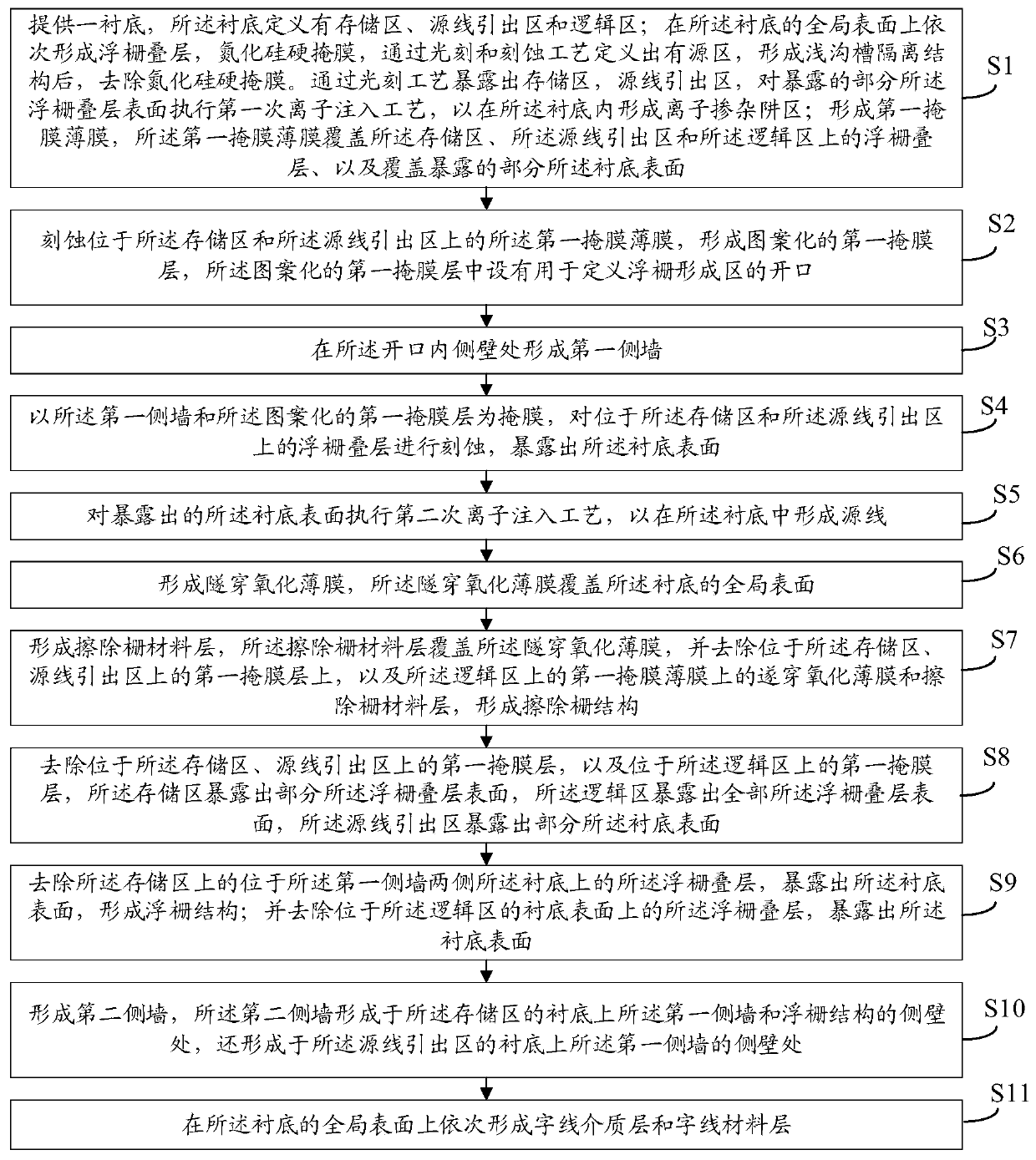
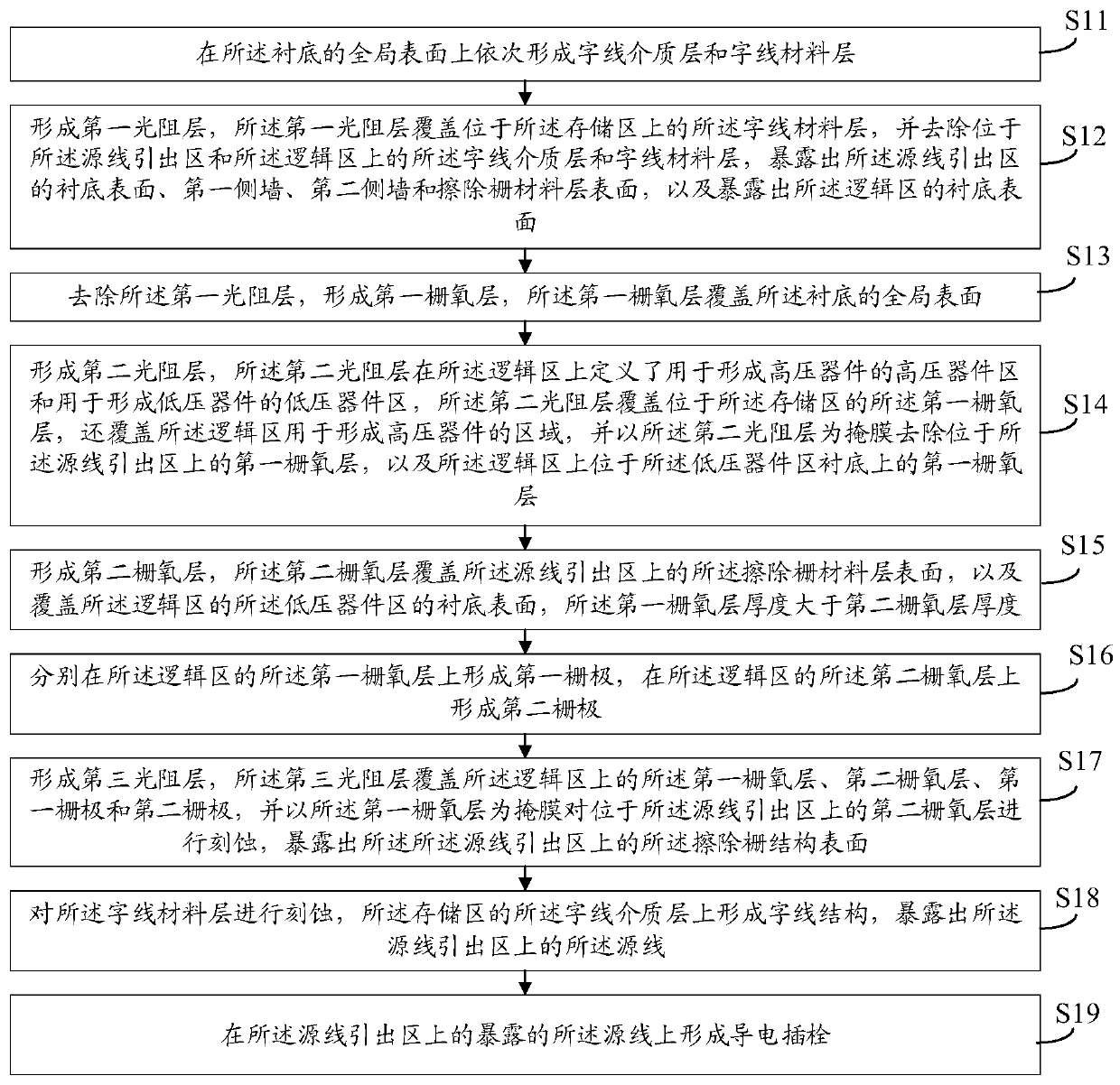
[0006] The purpose of the present invention is to provide a method for manufacturing embedded flash memory, which is used to solve the problem caused by the use of additional photomask and photolithography steps when preparing the conductive plug used to lead the source line out in the prior art. Improve the manufacturing cost of preparing the embedded flash memory and increase the complexity of its manufacturing process

Method used


Image

  • Manufacturing method of embedded flash memory
  • Manufacturing method of embedded flash memory
  • Manufacturing method of embedded flash memory

Examples


Embodiment Construction

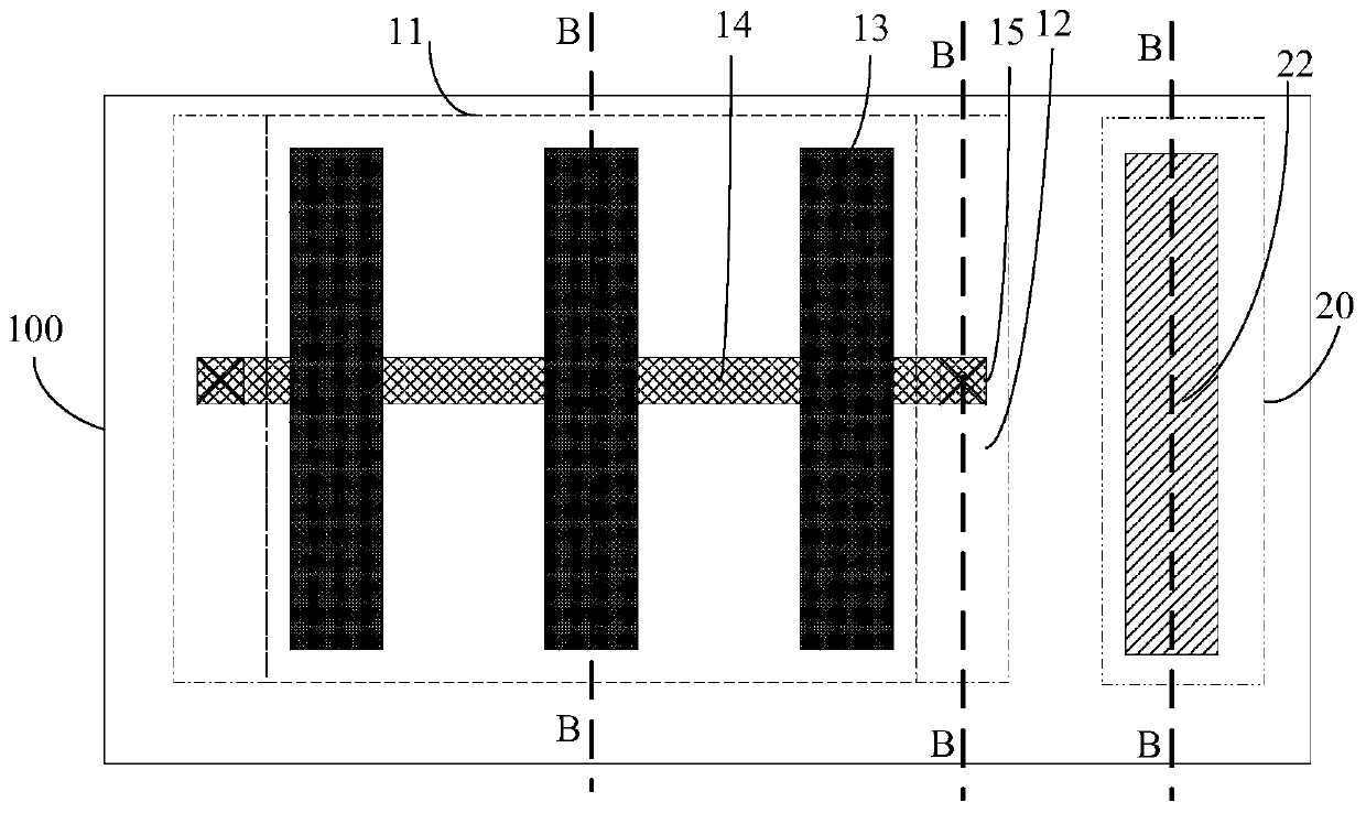
[0025] As described in the background, in the prior art, when preparing the conductive plug used to lead out the source line, additional photomasks and photolithography steps are used to increase the manufacturing cost of preparing the embedded flash memory. The problem of increasing the complexity of its manufacturing process is that the processes of memory cells (storage area) and logic transistors (logic area or peripheral area) are often performed on the same substrate at the same time. In the existing embedded flash memory manufacturing process, the embedded source line (Source line) is used as a buried layer under the erase gate (erase gate, EG) of the embedded flash memory, and the source line needs to use an additional Define the photomask with the pattern of the conductive plug leading out the source line, and remove the erasing gate material layer in the area used to form the conductive plug in combination with the photolithography process, The region forms a conduct...


PUM

PropertyMeasurementUnit
Thicknessaaaaaaaaaa
Thicknessaaaaaaaaaa

Abstract

The invention discloses a manufacturing method of an embedded flash memory. The method comprises the following steps: before forming a low-voltage device and a high-voltage device in a logic region, exposing the source line leading-out position of a source line leading-out region in an etching step of forming a word line in a storage region; during the formation of the grid electrode of the high-voltage device and / or the low-voltage device, by utilizing a protection layer of a first gate oxide layer, removing a first gate oxide layer on an erased gate structure above the source line leading-out position; generating a second gate oxide layer subsequently; utilizing the thickness difference between the first gate oxide layer and the second gate oxide layer, removing the second gate oxide layer and taking the remaining first gate oxide layer as a hard mask; removing one part of the erased gate structure above the source line; removing the remaining erased gate structure during the word line gate etching process and then forming a conductive plug to lead out the source line. In this way, the photoetching step of additionally leading out the source line and a photomask are omitted. Thepurposes of lowering the manufacturing cost of the embedded flash memory and lowering the complexity of the manufacturing process are achieved.

Description

technical field [0001] The invention relates to the technical field of semiconductor manufacturing, in particular to a method for manufacturing an embedded flash memory. Background technique [0002] In the current semiconductor industry, integrated circuit products can be mainly divided into three types: analog circuits, digital circuits and digital / analog hybrid circuits, among which storage devices are an important type of digital circuits. In recent years, among storage devices, the development of embedded flash memory (Embedded Flash Memory) is particularly rapid. The main feature of embedded flash memory is that it can keep stored information for a long time without power on; and it has the advantages of high integration, fast access speed, easy erasing and rewriting, etc. field has been widely used. [0003] Existing device structure prototypes of embedded flash memories include the following three types: a single-transistor memory cell based on a stacked gate struc...

Claims


Application Information

Patent Timeline
IPC IPC(8): H01L27/11531
CPCH10B41/42
Inventor 于涛
Owner SHANGHAI HUAHONG GRACE SEMICON MFG CORP
Learn More