Check patentability & draft patents in minutes with Patsnap Eureka AI!

Thinning method of III-V group semiconductor wafer

A III-V, semiconductor technology, used in semiconductor/solid-state device manufacturing, grinding machine components, and workpiece feed motion control, etc., can solve the problem of limited space for process parameter optimization, clogging of grinding fluid pipelines, and rough backside. In order to reduce the single-chip grinding time, increase the grinding rate, and reduce the operation risk

Inactive Publication Date: 2019-09-20
苏州长瑞光电有限公司
View PDF5 Cites 1 Cited by
  • Summary
  • Abstract
  • Description
  • Claims
  • Application Information

AI Technical Summary

Problems solved by technology

Analysis from the current process conditions: 1. The higher the pressure, the higher the grinding rate, but the wafer is easy to be fractured after the pressure is increased. In addition, the tray is not easy to rotate with the grinding disc after the pressure is increased, resulting in uneven grinding and prone to occurrence lobes
2. The faster the speed of the grinding disc, the higher the grinding rate; but limited by the equipment capacity, the current speed is close to the upper limit, and the optimization space is limited. 3. The larger the size of the grinding liquid particles, the stronger the cutting ability, so the higher the grinding rate; but use Large-grained abrasives are prone to cracks, and the roughness of the back surface will increase, reducing the chip's ability to withstand pressure
4. The higher the particle concentration of the grinding liquid, the faster the grinding rate, but the easier it is for the grinding liquid to solidify, thus blocking the grinding liquid pipeline
Taking a 4-inch gallium arsenide wafer as an example, the grinding rate under the current process conditions is about 10um / min. To reduce the original thickness of the 650um wafer to a thickness of 140~160um, the entire grinding time is about 50min, and the grinding rate low, grinding time is too long
[0006] Therefore, it is necessary to balance the grinding rate and grinding quality, and the current process parameter optimization space is limited, it is difficult to ensure product quality and effectively increase the grinding rate

Method used


Image

  • Thinning method of III-V group semiconductor wafer
  • Thinning method of III-V group semiconductor wafer
  • Thinning method of III-V group semiconductor wafer

Examples


Embodiment Construction

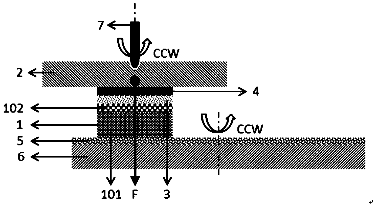
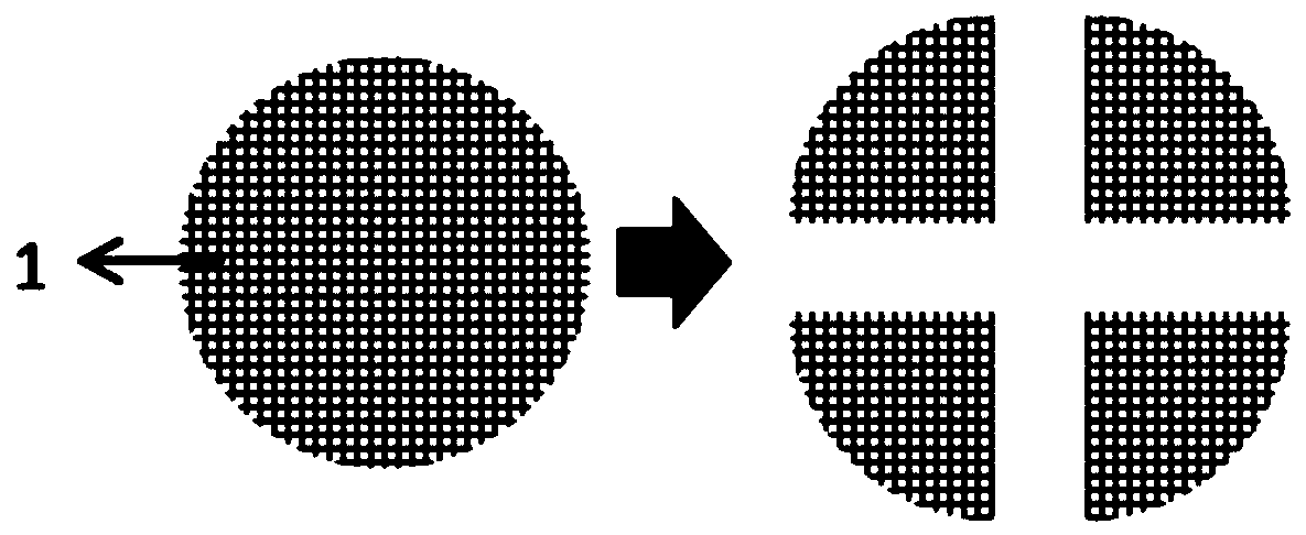
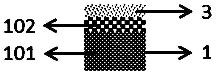
[0032] Aiming at the problem that the existing III-V semiconductor wafer thinning process is difficult to improve efficiency under the premise of ensuring quality, the present invention proposes a III-V semiconductor wafer that can improve production efficiency under the premise of ensuring quality Thinning method, by subdividing the whole wafer semi-finished product into pieces and performing back grinding to greatly increase the grinding rate; specifically, the III-V group semiconductor wafer has a plurality of device units divided by a plurality of dividing lines For the front side and the back side opposite to the front side, first divide the III-V group semiconductor wafer into a plurality of independent small wafers; then simultaneously grind the back sides of the plurality of independent small wafers, To reduce the thickness of the small wafer.

[0033] After a lot of experiments, the inventor found that: after the whole wafer is divided into multiple independent small ...


PUM


Abstract

The invention discloses a thinning method of an III-V group semiconductor wafer. The III-V group semiconductor wafer is provided with a front surface with multiple device units divided by multiple parting lines, and a back surface opposite to the front surface. The thinning method of the III-V group semiconductor wafer comprises the steps of firstly dividing the II-V group semiconductor wafer into multiple independent small wafer blocks; and then simultaneously grinding the back surfaces of the multiple independent small wafer blocks, so that the thickness of each small wafer block is thinned. Compared with the prior art, according to the thinning method of the III-V group semiconductor wafer provided by the invention, the grinding rate of the back surfaces of the wafers can be greatly improved, so that on the premise of ensuring the quality, the production efficiency can be improved.

Description

technical field [0001] The invention relates to a method for thinning III-V semiconductor wafers, belonging to the technical field of semiconductor device manufacturing. Background technique [0002] III-V group compound is a compound formed by B, Al, Ga, In of group III and N, P, As, Sb of group V in the periodic table of elements. The so-called group III-V semiconductor is composed of the above-mentioned group III The binary compound formed with group V elements has a chemical ratio of 1:1. III-V compound semiconductor materials have been widely used in optoelectronic devices, optoelectronic integration, ultra-high-speed microelectronic devices and ultra-high frequency microwave devices and circuits, and have broad prospects. The III-V semiconductors currently used in industry are mainly gallium arsenide (GaAs), indium phosphide (InP) and gallium nitride (GaN). [0003] In practical applications, III-V semiconductor devices generally need to be thinned to 50-200 um for h...

Claims


Application Information

Patent Timeline
IPC IPC(8): B24B37/10B24B37/005B24B49/00B24B57/02H01L21/304H01L21/78
CPCB24B37/005B24B37/107B24B49/006B24B57/02H01L21/304H01L21/78
Inventor 王鹤龙陆嘉鑫王国杰
Owner 苏州长瑞光电有限公司
Features
  • R&D
  • Intellectual Property
  • Life Sciences
  • Materials
  • Tech Scout
  • Unparalleled Data Quality
  • Higher Quality Content
  • 60% Fewer Hallucinations
Learn More