Preparation process for polysilicon film
A polysilicon thin film and preparation process technology, applied in polycrystalline material growth, metal material coating process, crystal growth, etc., can solve the problems of difficult crystallization of thin films, unfavorable thin film crystallization, long annealing time, etc., and achieve warpage The effect of low density, saving processing steps and reducing processing cost
- Summary
- Abstract
- Description
- Claims
- Application Information
AI Technical Summary
Problems solved by technology
Method used
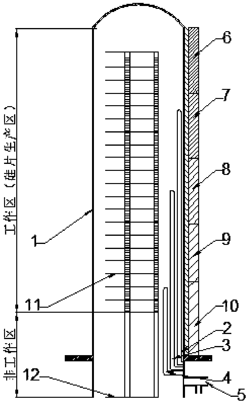
Image

Examples
Embodiment 1
[0036] 1. Process preparation:
[0037] 1. Raw materials: 150 pieces of 8-inch sour rot slices. There is no polysilicon film or oxide film on the surface of the sour rot slices, no surface cracks, no contamination, and no edge chipping or missing corners;
[0038] 2. Processing equipment: Telα-8s, DJ-853V;
[0039] 3. Measuring tool: ADE9600 automatic silicon wafer sorter;
[0040] 4. Excipients: SiH 4 , N 2 .
[0041] 2. The preparation process of polysilicon thin film is as follows:
[0042] Use a black PP basket to load the silicon wafer into the processing equipment, select the automatic upload mode, load the silicon wafer into the boat by the robot, and select the process 8000A, that is, the film thickness of the prepared polysilicon film is 800nm.
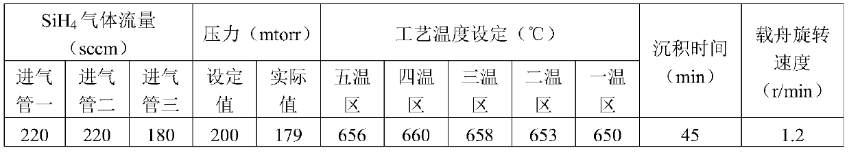
[0043] The specific process parameters are:
[0044]
Embodiment 2
[0046] 1. Process preparation:
[0047] 1. Raw materials: 150 pieces of 8-inch sour rot slices. There is no polysilicon film or oxide film on the surface of the sour rot slices, no surface cracks, no contamination, and no edge chipping or missing corners;
[0048] 2. Processing equipment: Telα-8s, DJ-853V;
[0049]3. Measuring tool: ADE9600 automatic silicon wafer sorter;
[0050] 4. Excipients: SiH 4 , N 2 .
[0051] 2. The preparation process of polysilicon thin film is as follows:
[0052] Use a black PP basket to load the silicon wafer into the processing equipment, select the automatic uploading mode, load the silicon wafer into the boat by the robot, and select the process 8000A, that is, the film thickness of the prepared polysilicon film is 800nm.
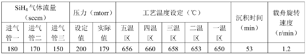
[0053] The specific process parameters are:
[0054]
PUM
| Property | Measurement | Unit |
|---|---|---|
| thickness | aaaaa | aaaaa |
Abstract
Description
Claims
Application Information
 - R&D
- Intellectual Property
- Life Sciences
- Materials
- Tech Scout
- Unparalleled Data Quality
- Higher Quality Content
- 60% Fewer Hallucinations
Browse by: Latest US Patents, China's latest patents, Technical Efficacy Thesaurus, Application Domain, Technology Topic, Popular Technical Reports.
© 2025 PatSnap. All rights reserved.Legal|Privacy policy|Modern Slavery Act Transparency Statement|Sitemap|About US| Contact US: help@patsnap.com