Silicon-based indium nitride solar cell and fabrication method thereof

A technology of solar cells and indium nitride, which is applied in the field of solar cells, can solve problems that have not been studied in depth, and achieve good application prospects, unique light confinement characteristics, and unique anti-reflection effects

Pending Publication Date: 2019-09-20
SHENZHEN KECHUANG DIGITAL DISPLAY TECH
View PDF0 Cites 0 Cited by
  • Summary
  • Abstract
  • Description
  • Claims
  • Application Information

AI Technical Summary

Problems solved by technology

Among them, indium nitride has excellent electron transport performance and narrow energy band, and has good application potential in optoelectronic devices, but the solar cells in the prior art have no idea how to improve the solar cell structure based on indium nitride materials and Improve its conversion efficiency, no in-depth study

Method used


Image

  • Silicon-based indium nitride solar cell and fabrication method thereof
  • Silicon-based indium nitride solar cell and fabrication method thereof

Examples


Embodiment 1

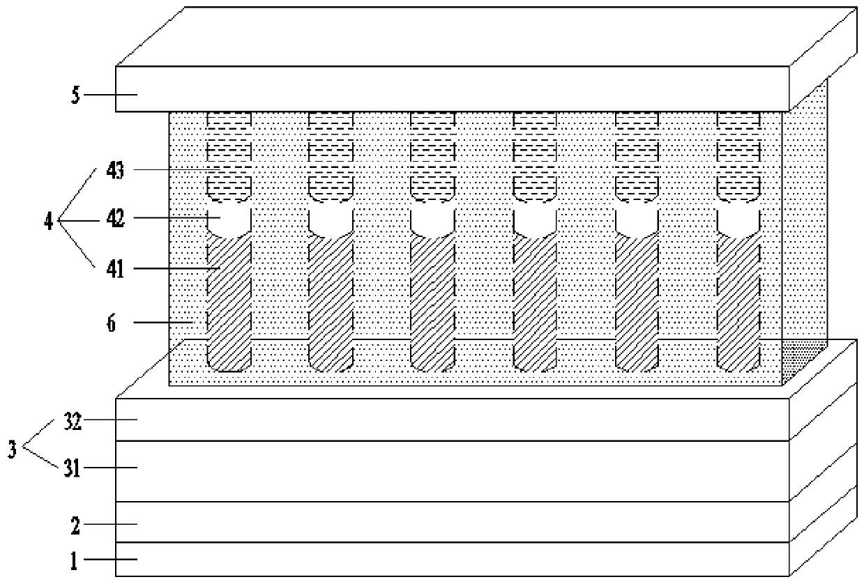
[0027] see figure 1 , the present embodiment provides a silicon-based indium nitride solar cell, including a negative electrode layer 1, a current diffusion layer 2, a Si sub-cell 3, multiple sets of columnar p-i-n type InN sub-cells 4 and a positive electrode layer 5, which are sequentially stacked. An insulating material 6 is filled between the positive electrode layer 5 and the Si sub-cell 3 to completely cover the columnar p-i-n type InN sub-cell 4 (in order to clearly see the internal structure of the solar cell, figure 1 The middle columnar p-i-n type InN subcell is indicated by the dashed line). In this embodiment, the negative electrode layer 1 is a Ti / Ag electrode, the current diffusion layer 2 is an ITO layer, the Si sub-cell 3 includes an n-type Si layer 31 and a p-type Si layer 32, and each columnar p-i-n type InN sub-cell 4 It consists of Si-doped n-type InN 41, undoped i-type InN42 and Mg-doped p-type InN 43 arranged in sequence, the positive electrode layer 5 i...


PUM

PropertyMeasurementUnit
diameteraaaaaaaaaa
lengthaaaaaaaaaa
diameteraaaaaaaaaa

Abstract

The invention discloses a silicon-based indium nitride solar cell and a fabrication method thereof. The silicon-based indium nitride solar cell comprises a negative electrode layer, a current diffusion layer, a Si sub-cell, at least one columnar p-i-n type InN sub-cell and a positive electrode layer which are sequentially arranged in a lamination way, wherein an insulation material is filled between the positive electrode layer and the Si sub-cell so as to completely cover the columnar p-i-n type InN sub-cell. Compared with a traditional PN-structure indium nitride cell, the p-i-n type indium nitride cell structure can allow more effective carrier generation due to the increment and presence of an intrinsic region (i layer) of indium nitride, so that the silicon-based indium nitride solar cell has relatively good conversion efficiency and has a relatively good application prospect in the field of solar cells.

Description

technical field [0001] The invention relates to the field of solar cells, in particular to a silicon-based indium nitride solar cell and a preparation method thereof. Background technique [0002] Nitride semiconductor materials are adjustable in a wide range of electron motion, so the energy band width range is large, and the band gap is significantly larger than that of Si and other semiconductor materials. It has important applications in many fields such as transistors, new solar cells, and semiconductor lighting. Among them, indium nitride has excellent electron transport performance and narrow energy band, and has good application potential in optoelectronic devices, but the solar cells in the prior art have no idea how to improve the solar cell structure based on indium nitride materials and Improving its conversion efficiency has not been studied in depth. Contents of the invention [0003] The object of the present invention is to provide a silicon-based indium n...

Claims


Application Information

Patent Timeline
Patent Type & Authority Applications(China)
IPC IPC(8): H01L31/0304H01L31/0352H01L31/075H01L31/18
CPCH01L31/03044H01L31/035281H01L31/075H01L31/1876Y02E10/544Y02E10/548Y02P70/50
Inventor 郭建廷李方红常嘉兴
Owner SHENZHEN KECHUANG DIGITAL DISPLAY TECH
Why Eureka
Try Eureka