Power chip pre-packaging method and structure, power chip packaging method and structure and wafer pre-packaging structure
A power chip and packaging structure technology, which is applied in the manufacture of electrical components, electrical solid devices, semiconductor/solid devices, etc., can solve the problems of low reliability of devices, pollution of chip terminals, etc., to improve quality, avoid pollution, and save packaging links and cost effects
- Summary
- Abstract
- Description
- Claims
- Application Information
AI Technical Summary
Problems solved by technology
Method used
Image
Examples
Embodiment 1
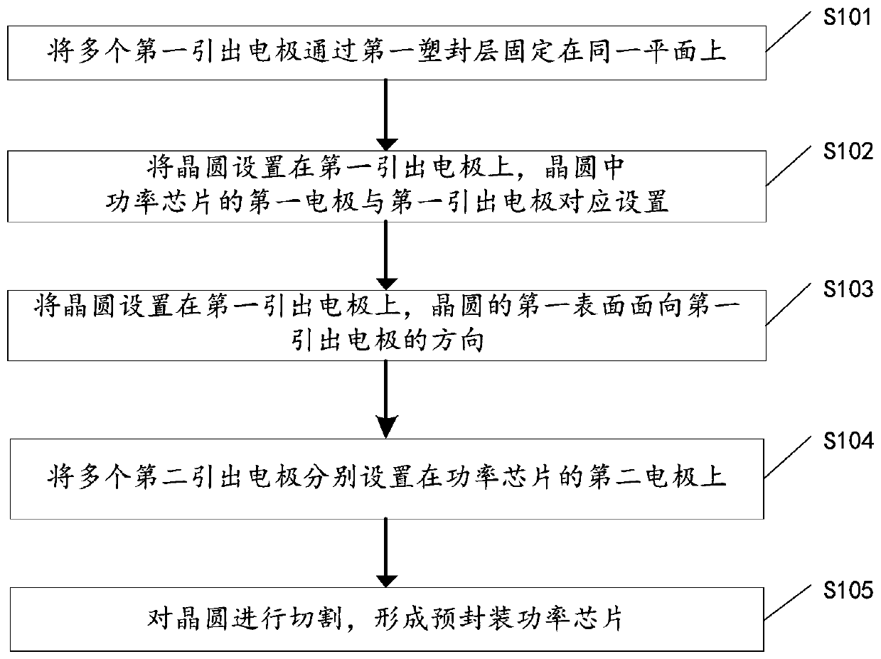
[0030] An embodiment of the present invention provides a power chip prepackaging method, which is used for a wafer, and a plurality of power chips are arranged in an array on the wafer, the first electrode of the power chip is located on the first surface of the wafer, and the second electrode of the power chip Located on the second surface of the wafer, the power chip can be any one of double insulated gate transistors, fast recovery diodes and silicon carbide metal-oxide semiconductor field effect transistors. When the power chip is an IGBT, the first electrode may be a collector of the power chip. Such as figure 1 As shown, the power chip prepackaging method includes the following steps:
[0031]S101: Fix the multiple first lead-out electrodes 11 on the same plane through the first encapsulation layer 21 . Specifically, packaging material can be used to fill the spaces between the first extraction electrodes 11 to form a first packaging layer 21 surrounding the first extr...
Embodiment 2
[0039] The embodiment of the present invention also provides a power chip packaging method, the power chip packaging method includes the following steps:
[0040] The prepackaged power chip obtained according to the power chip prepackaging method described in Embodiment 1 is packaged by a crimping package process.
[0041] When the pre-packaged power chip is packaged by the press-fit packaging process, such as image 3 As shown, the pre-packaged power chip 100 can be packed into the packaging shell 200, and placed on the boss of the lower cover 400, and the upper cover 300 is applied on top, so as to complete the packaging of the press-fit power device.
[0042] In the power chip packaging method provided by the embodiment of the present invention, when the pre-packaged power chip is packaged by using the crimping packaging process, since the power chip is pre-packaged, the power chip is protected from the influence of the packaging process to the greatest extent. Therefore, ...
Embodiment 3
[0044] The embodiment of the present invention also provides a wafer pre-packaging structure, such as Figure 2D As shown, the wafer pre-packaging structure includes: a wafer 4, the wafer 4 includes a plurality of power chips 42 arranged in an array, the first electrode 43 of the power chip 42 is located on the first surface of the wafer, and the first electrode 43 of the power chip 42 Two electrodes 41 are located on the second surface of the wafer; a plurality of first lead-out electrodes 11 are respectively connected to the first electrodes 43; the first encapsulation layer 21 fills the space between each first lead-out electrodes 11, and is connected to the wafer The first surface of 4 is separated; a plurality of second extraction electrodes 12 are connected to the second electrodes 41 respectively; the second encapsulation layer 22 fills the space between each second extraction electrodes 12 .
[0045] The wafer pre-packaging structure provided by the embodiment of the p...
PUM
 Abstract
Description
Claims
Application Information
 - R&D
- Intellectual Property
- Life Sciences
- Materials
- Tech Scout
- Unparalleled Data Quality
- Higher Quality Content
- 60% Fewer Hallucinations
Browse by: Latest US Patents, China's latest patents, Technical Efficacy Thesaurus, Application Domain, Technology Topic, Popular Technical Reports.
© 2025 PatSnap. All rights reserved.Legal|Privacy policy|Modern Slavery Act Transparency Statement|Sitemap|About US| Contact US: help@patsnap.com


