Semiconductor device chip structure and preparation method thereof

A device chip and semiconductor technology, which is applied in the field of semiconductor device chip structure and its preparation, can solve the problems of low preparation efficiency, and achieve the effects of simplifying the preparation process, improving the performance and improving the preparation time.

Inactive Publication Date: 2019-09-24
INST OF SEMICONDUCTORS - CHINESE ACAD OF SCI
View PDF2 Cites 2 Cited by
  • Summary
  • Abstract
  • Description
  • Claims
  • Application Information

AI Technical Summary

Problems solved by technology

The existing method for preparing the chip structure of semiconductor devices is very operable, and devices with good performance can be obtained, but the preparation efficiency is low

Method used


Image

  • Semiconductor device chip structure and preparation method thereof
  • Semiconductor device chip structure and preparation method thereof
  • Semiconductor device chip structure and preparation method thereof

Examples


preparation example Construction

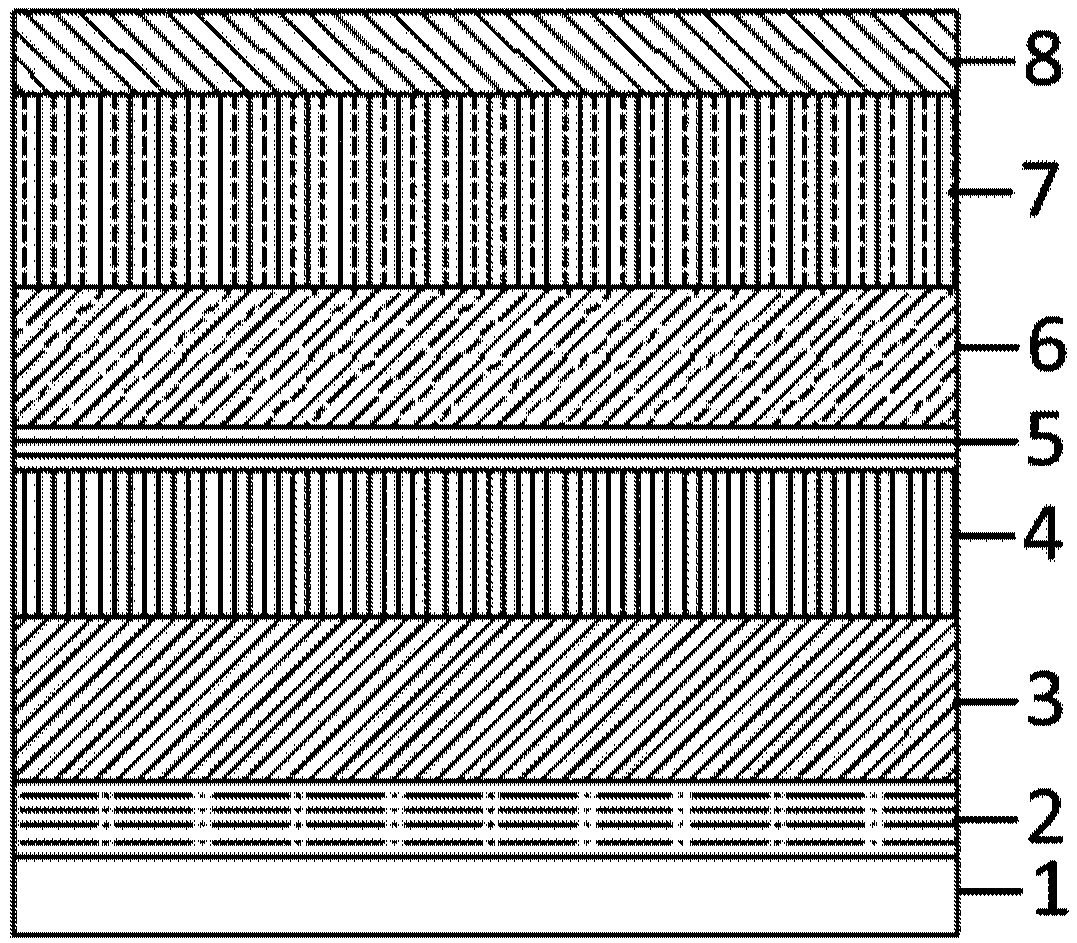
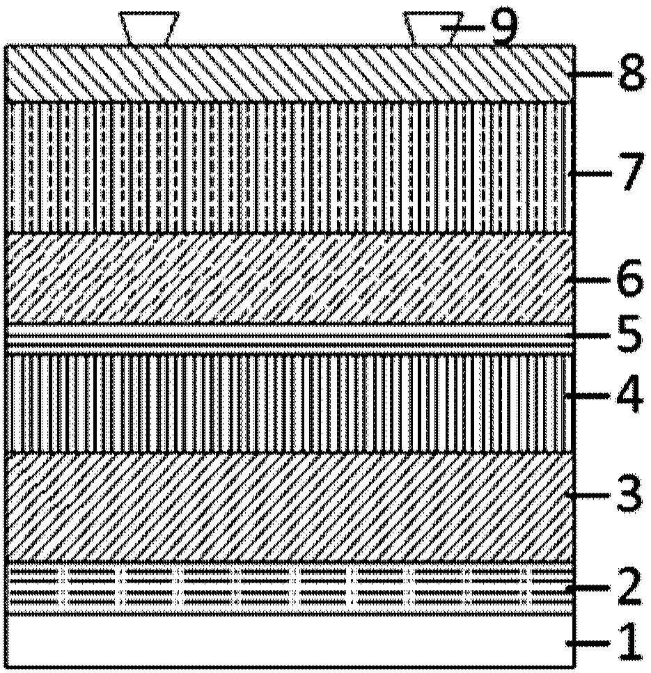
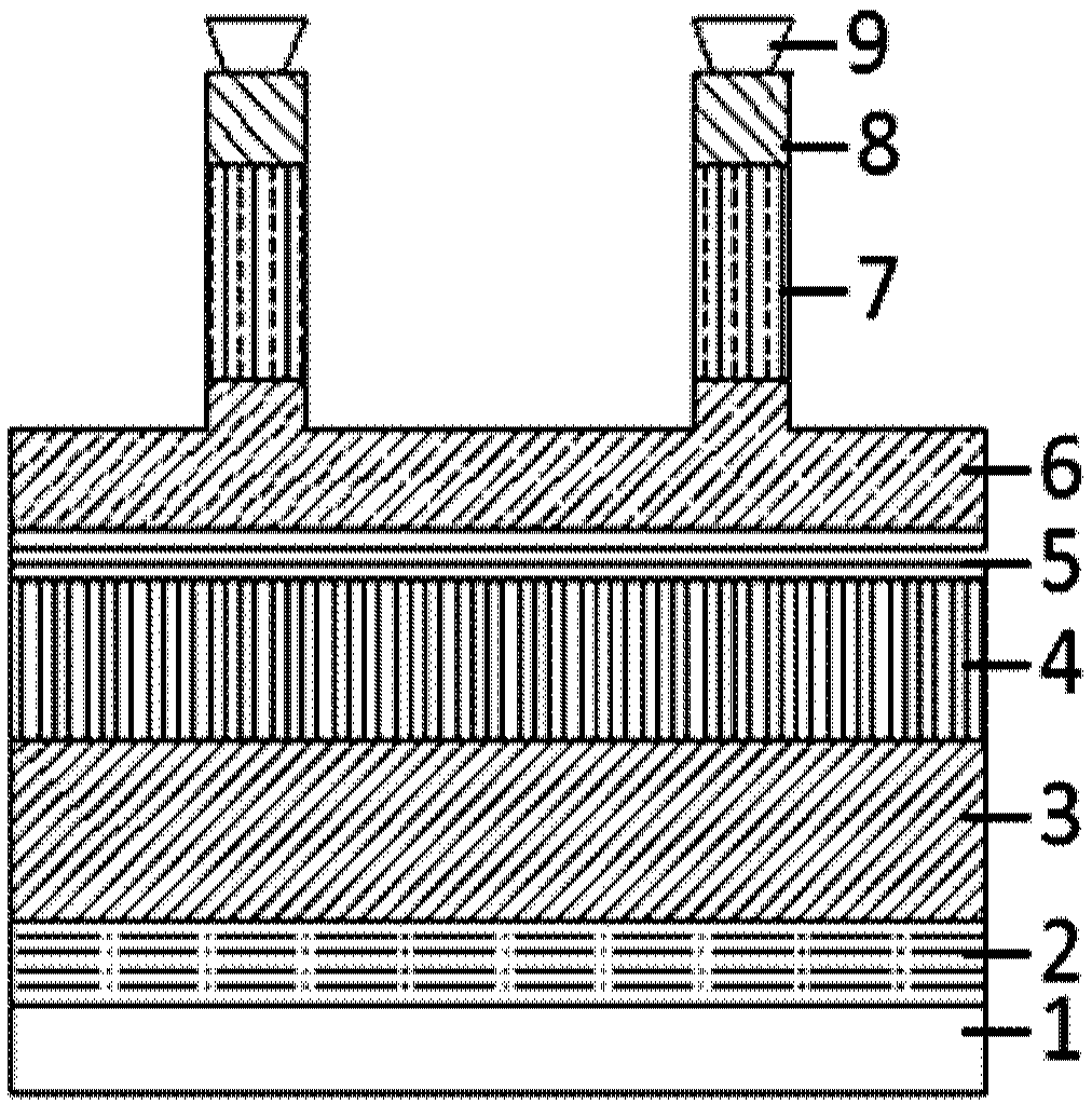
[0031] The present disclosure discloses a method for preparing a chip structure of a ridge-shaped mesa semiconductor device, comprising the following steps:

[0032] S1. Form a photoresist mask on the semiconductor epitaxial wafer, and develop it to form a periodic structure after exposure by a photolithography machine;

[0033] S2. Dry or wet etching to remove part of the epitaxial layer in the masked area without photoresist, and form a ridge-shaped mesa structure on the semiconductor epitaxial wafer;

[0034] S3, depositing a layer of electrical insulating medium on the surface of the semiconductor epitaxial wafer;

[0035] S4. Using an organic solvent to remove the photoresist on the ridge-shaped mesa and the electrical insulating medium on the photoresist to make a current injection window.

[0036] S5, evaporating and sputtering the P-type electrode, thinning the substrate, sputtering the N-type electrode, evaporating the alloy, and completing the preparation of the chi...


PUM

PropertyMeasurementUnit
Thicknessaaaaaaaaaa

Abstract

The invention provides a semiconductor device chip structure and a preparation method thereof. The preparation method of the semiconductor device chip structure comprises the steps of forming a photoresist mask on a semiconductor epitaxial wafer, and developing after exposure to form a periodic structure; etching to remove part of the epitaxial layer without a photoresist masking area, and forming a ridge-shaped mesa structure on the semiconductor epitaxial wafer; depositing an electrical insulation dielectric layer on the surface of the semiconductor epitaxial wafer with the ridge-shaped mesa structure; removing the electrical insulation dielectric on the ridge-shaped mesa, and manufacturing a current injection window; and forming a P-type electrode and an N-type electrode on the semiconductor epitaxial wafer so as to complete the preparation of the semiconductor device chip structure. The semiconductor device chip structure and the preparation method thereof simplify the preparation process of the semiconductor device and improve the preparation time efficiency under the premise of ensuring good device performance.

Description

technical field [0001] The disclosure belongs to the technical field of semiconductor optoelectronics, and in particular relates to a semiconductor device chip structure and a preparation method thereof. Background technique [0002] Semiconductor devices, such as semiconductor lasers, are one of the core technologies of optoelectronic practical devices today. They have the advantages of small size, light weight, and long life, and are widely used in civilian production and military fields. Existing semiconductor lasers are usually coated with photoresist 2 to 3 times in the preparation process, using the photoresist as a mask, and using an etching solution to etch the epitaxial wafer to form a mesa; the silicon dioxide is grown on it by etching Or silicon carbide and other insulating media to form a current injection window. The existing method for preparing a chip structure of a semiconductor device is highly operable and can obtain a device with good performance, but the...

Claims


Application Information

Patent Timeline
IPC IPC(8): H01S5/22H01S5/32
CPCH01S5/22H01S5/32
Inventor 曼玉选祁琼彭岩刘素平马骁宇
Owner INST OF SEMICONDUCTORS - CHINESE ACAD OF SCI
Why Eureka
Try Eureka