Method for manufacturing solder mask layer of circuit board

A production method and circuit board technology, which is applied in the fields of printed circuit manufacturing, printed circuit, printed circuit secondary treatment, etc., can solve the problems of low pass rate, high energy consumption, complicated process, etc., and achieve simple process flow and ecological protection Environment, improve the effect of ion pollution

Active Publication Date: 2019-10-22
深圳明阳电路科技股份有限公司
View PDF6 Cites 8 Cited by
  • Summary
  • Abstract
  • Description
  • Claims
  • Application Information

AI Technical Summary

Problems solved by technology

This process of making solder mask has the following disadvantages: as figure 1 As shown, the solder resist 4' on the edge of the circuit 2 on the circuit board base material 1 is relatively thin, and the thickness of the solder resist 4' on the edge of the circuit 2 is usually only 5-7um after printing once; Undercut5' appears at the window opening of the solder resist, which leads to the problem of ion pollution on the circuit board; the process of exposing and developing requires high energy consumption, and the process is complicated, and the pass rate is not high; the process of developing requires water, And a lot of sewage is generated; the ability of the solder resist bridge between line 2 and pad 3 is limited. Usually, for the outer HOZ bottom copper, to realize the design and manufacture of solder resist bridge between the pads, the spacing between the pads needs to be about 7mil , for the more and more densely designed circuit boards, the traditional process is facing great challenges; for circuit boards with dense lines, there are often defects on the pads on the solder mask oil printing, and the accuracy is not high
Although this can increase the thickness of the solder resist oil on the edge of the line, there are still the following defects: there are two layers of solder resist oil on the edge of the line, which makes the solder resist oil uneven and affects the appearance; the ink coverage on the edge of the line is not tight, and there are holes. During laser window opening and edge trimming, the laser may burn onto the substrate, resulting in cloth lines on the circuit board

Method used


Image

  • Method for manufacturing solder mask layer of circuit board
  • Method for manufacturing solder mask layer of circuit board
  • Method for manufacturing solder mask layer of circuit board

Examples


Embodiment 1

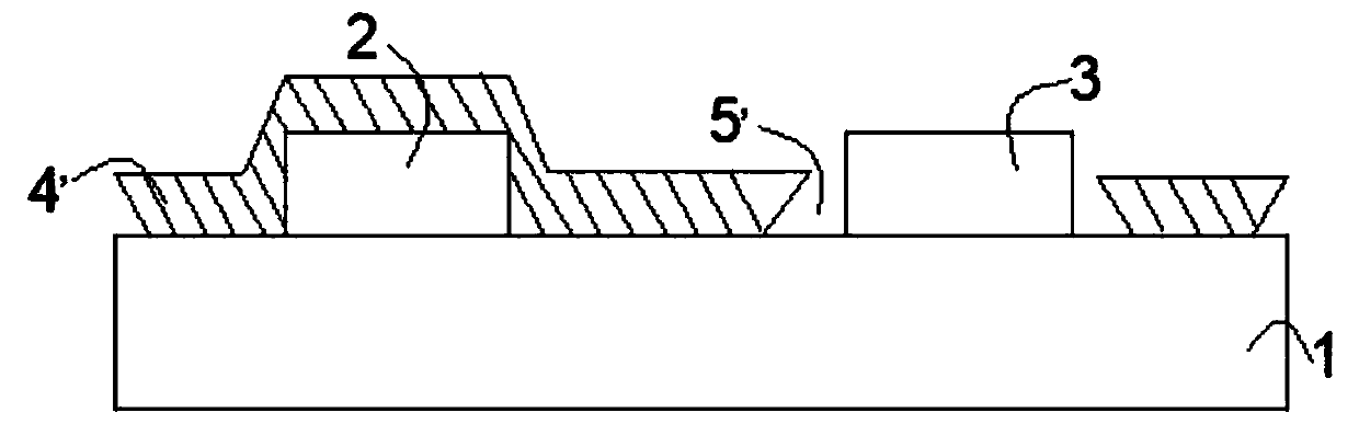
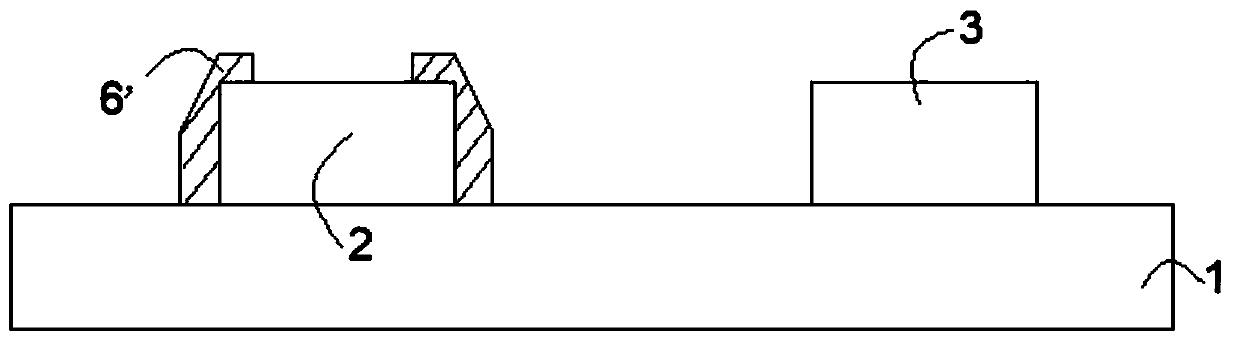
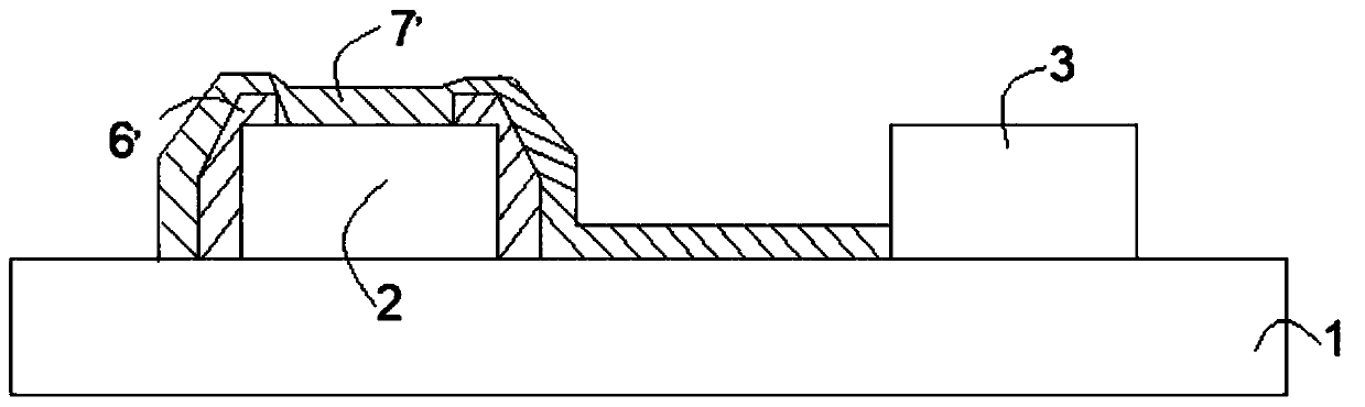
[0048] A method for manufacturing a circuit board solder mask, comprising the following steps in turn:

[0049] Filling ink: According to the information of CAM, printing technology is used to print the ink pattern between the circuit board and the pad, and cure the ink pattern with ultraviolet light; the filled ink is resin ink material; the thickness of the filled ink is the thickness of the line 50% of.

[0050] Pre-treatment of solder resist: including the step of grinding the plate; the step of grinding the plate is to use a grinding roller to grind off the ink dripping on the circuit and pad surface of the circuit board;

[0051] Solder masking steps: cover solder resist oil on the circuit board after solder mask pre-treatment; cover solder mask oil is based on CAM data, use printing technology to print the pattern of solder mask oil, and use the printed solder mask oil pattern UV light curing. On the substrate surface of the circuit board, after the solder resist is p...

Embodiment 2

[0056] A method for manufacturing a circuit board solder mask, comprising the following steps in turn:

[0057] Filling ink: According to the information of CAM, printing technology is used to print the ink pattern between the circuit board and the pad, and cure the ink pattern with ultraviolet light; the filled ink is resin ink material; the thickness of the filled ink is the thickness of the line 95% of.

[0058] Pre-treatment of solder resist: including the step of grinding the plate; the step of grinding the plate is to use a grinding roller to grind off the ink dripping on the circuit board and the surface of the pad;

[0059] Solder masking steps: cover solder resist oil on the circuit board after solder mask pre-treatment; cover solder mask oil is based on CAM data, use printing technology to print the pattern of solder mask oil, and use the printed solder mask oil pattern UV light curing. On the substrate surface of the circuit board, after the solder resist is print...

Embodiment 3

[0064] A method for manufacturing a circuit board solder mask, comprising the following steps in turn:

[0065] Filling ink: According to the information of CAM, printing technology is used to print the ink pattern between the circuit board and the pad, and cure the ink pattern with ultraviolet light; the filled ink is resin ink material; the thickness of the filled ink is the thickness of the line 65% of.

[0066] Pre-treatment of solder resist: including the step of grinding the plate; the step of grinding the plate is to use a grinding roller to grind off the ink dripping on the circuit and pad surface of the circuit board;

[0067] Solder masking steps: cover solder resist oil on the circuit board after solder mask pre-treatment; cover solder mask oil is based on CAM data, use printing technology to print the pattern of solder mask oil, and use the printed solder mask oil pattern UV light curing. On the substrate surface of the circuit board, after the solder resist is p...


PUM


Abstract

The invention discloses a method for manufacturing a solder mask layer of a circuit board. The method comprises the following steps of: an ink filling step: filling the space between a circuit and a bonding pad of the circuit board with ink; a solder mask pre-processing step: performing solder mask pre-processing on the circuit board after the ink filling step; a solder mask step: covering the circuit board subjected to the solder mask pretreatment step with solder mask oil; and a curing step: carrying out curing treatment on the circuit board subjected to the solder mask step. According to the invention, the thickness of the solder mask oil of the circuit edge of the circuit board can meet the requirements, and the surface of the solder mask layer can be smooth and beautiful; and meanwhile, cloth marks are not exposed when laser windowing and trimming are carried out on the circuit board.

Description

technical field [0001] The invention relates to the technical field of circuit board production, in particular to a method for producing a circuit board solder mask. Background technique [0002] Circuit board, also known as circuit board or printed circuit board, is one of the important components of the electronics industry, a support for electronic components, and a carrier for electrical connections. The production process of the circuit board includes the following steps in turn: opening the board, making the inner layer circuit, pressing, drilling, sinking copper, electroplating the whole board, making the outer layer circuit, making the solder mask, surface treatment, and forming. Among them, making the solder mask refers to coating a layer of solder mask ink on the circuit board after the outer layer of the circuit is made, except for the pads and holes used for welding, so as to protect and prevent the circuit board. role of welding. [0003] In the prior art, the...

Claims


Application Information

Patent Timeline
Patent Type & Authority Applications(China)
IPC IPC(8): H05K3/28
CPCH05K3/282
Inventor 张佩珂胡诗益
Owner 深圳明阳电路科技股份有限公司
Why Eureka
Try Eureka