

Display substrate and preparation method thereof and display device
A display substrate and substrate substrate technology, applied in semiconductor/solid-state device manufacturing, semiconductor devices, electrical components, etc., can solve the problem of fast solvent evaporation rate, uneven film thickness of pixel ink, impact on display device life and display effect, etc. question
- Summary
- Abstract
- Description
- Claims
- Application Information
AI Technical Summary
Problems solved by technology
Method used
Image

Examples
no. 1 example
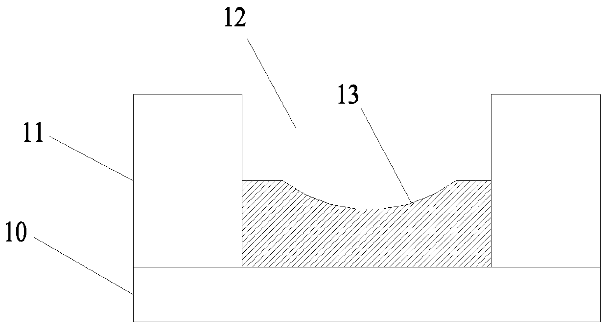
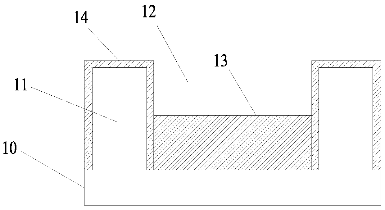
[0034] figure 2 It is a cross-sectional view showing a film of pixel ink in a substrate according to an embodiment of the present invention. Such as figure 2 As shown, the display substrate in the embodiment of the present invention includes a base substrate 10, on which a pixel defining layer 11 is arranged, and a pixel region 12 for accommodating pixel ink is formed between the pixel defining layers 11, and between the pixel defining layers 11 A light-to-heat conversion layer 14 for converting light energy into heat energy is arranged on it.
[0035] Such as figure 2 As shown, in this embodiment, the substrate is dripped with pixel ink in the pixel area 12, and then the pixel ink in the pixel area 12 is heated, and at the same time, the light-to-heat conversion layer 14 on the pixel defining layer 11 is irradiated by light, The light-to-heat conversion layer 14 converts the light energy irradiated thereon into heat energy, and uses the heat energy formed by light energ...
no. 2 example
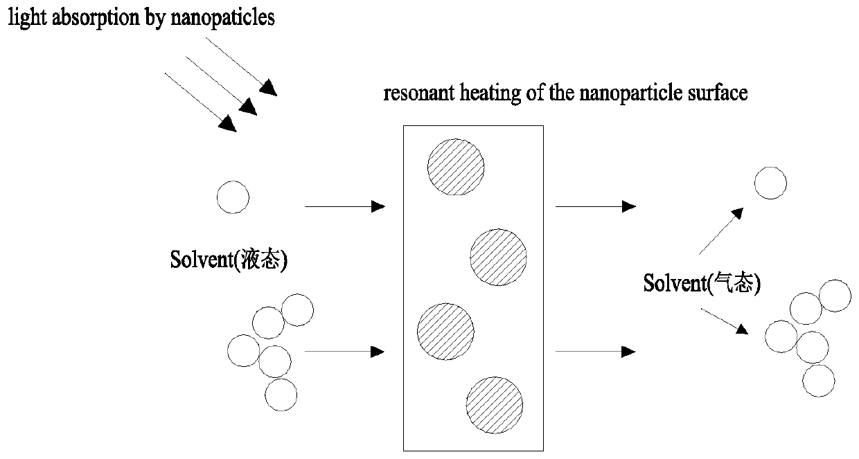
[0042] Figure 4 A schematic diagram showing the structure of core-shell nanoparticles in a substrate for an embodiment of the present invention. Such as Figure 4 As shown, this embodiment is an extension of the aforementioned first embodiment. This embodiment shows that the material of the light-to-heat conversion layer in the substrate includes core-shell nanoparticles 15, and the core-shell nanoparticles 15 include a light-to-heat conversion material core 151 and A hydrophobic material shell 152 wrapped on the outer surface of the light-to-heat conversion material core 151 .
[0043] In the embodiment, the material of the core of the light-to-heat conversion material and the material of the shell of the hydrophobic material are not limited, as long as the material of the core of the light-to-heat conversion material can convert light energy into heat energy, and the material of the shell of the hydrophobic material can form the light-to-heat conversion layer A hydrophobi...
no. 3 example
[0046] Based on the technical idea of the foregoing embodiments, the embodiments of the present invention further provide a method for preparing a display substrate, so as to prepare the display substrate of the foregoing embodiments.
[0047] Figure 5 A flowchart showing a method for preparing a substrate is an embodiment of the present invention. Such as Figure 5 As shown, the embodiment of the present invention shows that the preparation method of the substrate includes:
[0048] 1) A pixel defining layer is formed on the base substrate, and a pixel area for accommodating pixel ink is formed between the pixel defining layers;
[0049] 2) forming a light-to-heat conversion layer for converting light energy into heat energy on the pixel defining layer;
[0050] 3) dripping pixel ink into the above pixel area;
[0051] 4) Heating the pixel ink in the above-mentioned pixel area, and irradiating the above-mentioned light-to-heat conversion layer with light; so that the l...
PUM
 Abstract
Description
Claims
Application Information