Supercharge Your Innovation With Domain-Expert AI Agents!

Copper-indium-gallium-selenium solar cell module and manufacturing method thereof

A solar cell, copper indium gallium selenide technology, applied in electrical components, circuits, photovoltaic power generation and other directions, can solve the problems of low transmittance, difficult preparation, high maintenance cost, improve conversion efficiency, improve light transmittance and The effect of conductivity

Pending Publication Date: 2019-11-05
上海祖强能源有限公司
View PDF0 Cites 2 Cited by
  • Summary
  • Abstract
  • Description
  • Claims
  • Application Information

AI Technical Summary

Problems solved by technology

[0004] AZO film is usually prepared by vacuum magnetron sputtering coating equipment, which occupies a relatively large space, and the equipment price is high, and the maintenance cost is high
On the other hand, limited by the negative correlation between the conductivity and light transmittance of AZO itself, that is, the greater the thickness of AZO, the better the conductivity, but at the same time the lower the transmittance, resulting in the current process conditions, the thickness of AZO needs to be Reaching 800~1200nm can take into account better conductivity and transmittance
In addition, the film properties of AZO depend on the structure and components of the AZO target, and require a reliable and stable preparation process, which requires high preparation technology and is difficult to prepare

Method used


Image

  • Copper-indium-gallium-selenium solar cell module and manufacturing method thereof
  • Copper-indium-gallium-selenium solar cell module and manufacturing method thereof
  • Copper-indium-gallium-selenium solar cell module and manufacturing method thereof

Examples


Embodiment Construction

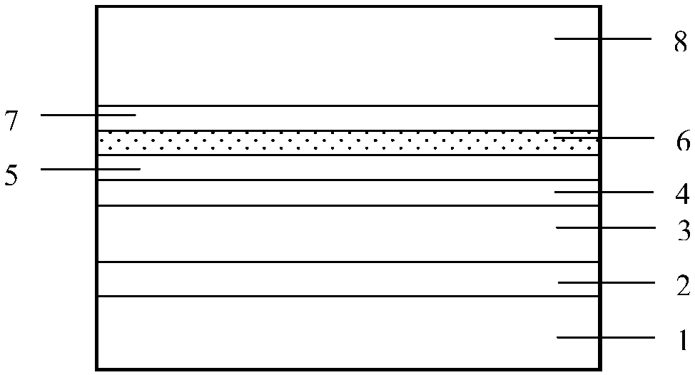
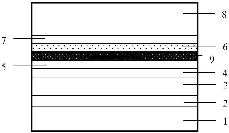
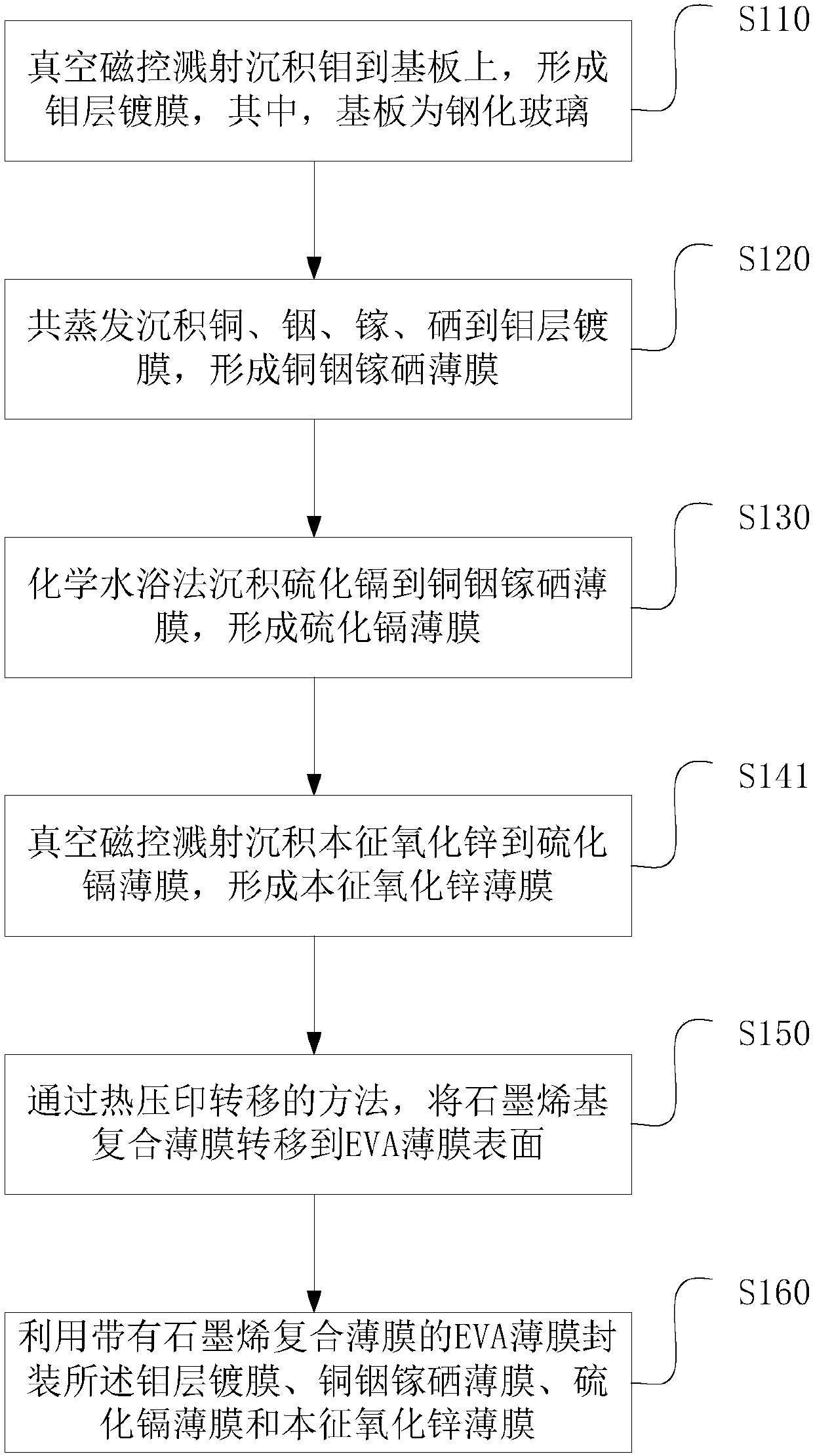
[0038] In order to make the purpose, technical solutions and advantages of the embodiments of the present invention clearer, the technical solutions in the embodiments of the present invention will be clearly and completely described below in conjunction with the drawings in the embodiments of the present invention. Obviously, the described embodiments It is a part of embodiments of the present invention, but not all embodiments. Based on the embodiments of the present invention, all other embodiments obtained by persons of ordinary skill in the art without making creative efforts belong to the protection scope of the present invention.

[0039] In the following detailed description, reference is made to the accompanying drawings which are included in the specification and which illustrate specific embodiments of the application and which are included in this application. In the drawings, like reference numerals describe substantially similar components in different views. Va...


PUM

PropertyMeasurementUnit
Thicknessaaaaaaaaaa
Thicknessaaaaaaaaaa
Thicknessaaaaaaaaaa

Abstract

The invention relates to a copper-indium-gallium-selenium solar cell module and a manufacturing method thereof. The copper-indium-gallium-selenium solar cell module comprises a substrate, a back electrode, a light absorption layer, a buffer layer and a window layer, wherein the back electrode is arranged on the substrate; the light absorption layer is arranged on the back electrode; the buffer layer is arranged on the light absorption layer; the window layer is arranged on the buffer layer, wherein the window layer comprises a high resistance layer and a transparent conductive layer; the transparent conductive layer comprises a graphene-based composite thin film arranged on the high resistance layer. According to the copper-indium-gallium-selenium solar cell module provided by the embodiment of the invention, the graphene-based thin film is introduced into the CIGS thin-film solar preparation process to serve as the transparent conductive layer, the light transmittance of the graphene-based composite thin film can reach 94%, and meanwhile, the resistivity is lower than 8 omega / sq, so that the light transmittance and the conductivity of the transparent conductive layer of the CIGS thin-film solar cell module are effectively improved, and the conversion efficiency of the copper-indium-gallium-selenium solar cell module is improved.

Description

technical field [0001] The invention relates to the technical field of thin film solar cells, in particular to a copper indium gallium selenium solar cell component and a manufacturing method thereof. Background technique [0002] Copper indium gallium selenide (CIGS) thin film solar cell modules usually use aluminum zinc oxide (AZO) as a transparent conductive layer (TCO) as the front electrode of the battery chip to collect the photocurrent generated by the battery. The position of AZO layer in CIGS thin film solar cell module, such as figure 1 Shown in 6. In order to improve the conversion efficiency of CIGS thin-film solar cell modules, the AZO layer is required to have both high light transmittance and low resistivity. [0003] AZO is usually prepared using vacuum magnetron sputtering coating equipment, according to Al 2 o 3 Depending on the doping concentration and the magnetron sputtering preparation process, the transmittance and resistivity of the AZO layer are ...

Claims


Application Information

Patent Timeline
IPC IPC(8): H01L31/0749H01L31/0224H01L31/18
CPCH01L31/0749H01L31/022466H01L31/18Y02E10/541Y02P70/50
Inventor 赵树利杨立红叶亚宽王磊
Owner 上海祖强能源有限公司
Features
  • R&D
  • Intellectual Property
  • Life Sciences
  • Materials
  • Tech Scout
  • Unparalleled Data Quality
  • Higher Quality Content
  • 60% Fewer Hallucinations
Learn More