High-power semiconductor laser array wavelength locking and line width compression device and method

A laser array and wavelength locking technology, applied in the field of lasers, can solve problems such as restricting power expansion capabilities and increasing system complexity, and achieve the effects of facilitating industrialization and large-scale application, simple and effective power expansion, and reducing quantity requirements

Pending Publication Date: 2019-11-15
NAT UNIV OF DEFENSE TECH
View PDF0 Cites 5 Cited by
  • Summary
  • Abstract
  • Description
  • Claims
  • Application Information

AI Technical Summary

Problems solved by technology

Such a structure greatly increases the complexity of the sy

Method used


Image

  • High-power semiconductor laser array wavelength locking and line width compression device and method

Examples


Example Embodiment

[0030] In order to make the object, technical solution and advantages of the present invention clearer, the present invention will be further described in detail below in conjunction with the accompanying drawings and embodiments. It should be understood that the specific embodiments described here are only used to explain the present invention, not to limit the present invention.

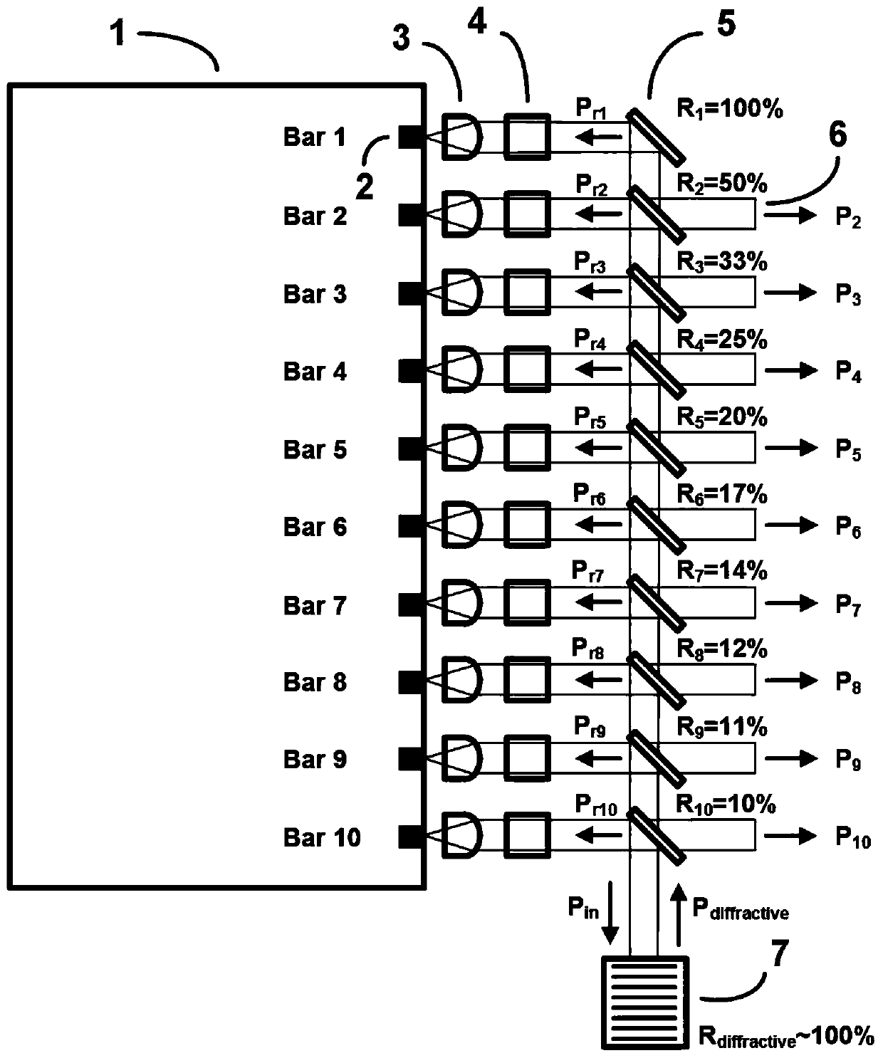
[0031] refer to figure 1 In this embodiment, a vertically stacked semiconductor laser array containing 10 bars is taken as an example for illustration. In the figure, 1 is the packaging and heat sink part of the semiconductor laser array, and 2 is the bar, that is, the laser emitting area. The semiconductor laser array includes n bars distributed in a one-dimensional array, n=10, in figure 1 In , respectively mark Bar 1, Bar 2...Bar 10 from top to bottom, and record the free-running output power of a single bar as P (usually in the order of ~100W).

[0032] The laser light directly emitted by eac...


PUM


Abstract

The invention discloses a high-power semiconductor laser array wavelength locking and line width compression device and a method. The device comprises a semiconductor laser array, a beam shaping system, a partial reflection mirror and a dispersion optical element. The laser emitted by each bar of the semiconductor laser array is collimated by the corresponding beam shaping system and then output in parallel. The parallel laser beams are respectively incident to the corresponding partial reflectors. One part of light in each laser beam is reflected by the corresponding partial reflector, then is sequentially reflected by other subsequent partial reflectors of the reflection light path and finally enters the dispersion optical element; diffracted light returns along an original path and enters each bar of the semiconductor laser array again after being reflected by each partial reflector, and each bar, the light beam shaping system corresponding to each bar, part of reflectors and the dispersion optical element form an external cavity structure together. According to the method, strict consistency of emergent wavelengths of different light emitting sources can be ensured, and accurate wavelength locking and ultra-narrow linewidth spectrum output are easy to realize.

Description

technical field [0001] The invention belongs to the technical field of lasers, and in particular relates to a novel high-power semiconductor laser array wavelength locking and line width compression device and method. Background technique [0002] With its high electro-optic conversion efficiency (usually ≥ 60%), light and compact volume structure, wide band coverage (0.6-2um) and scalable high power output capability (kW ~ 100kW), semiconductor lasers are widely used in industry and national defense. It has important applications in fields such as scientific research and medical treatment. [0003] The wavelength of the emitted laser light of conventional semiconductor lasers has a certain deviation (±3nm) from the nominal value, and the center wavelength will drift with the change of driving current and temperature, usually in the range of 0.2-0.3nm / A (nm / K), Its typical emission spectrum linewidth is 3-5nm (FWHM), and the above indicators can generally meet the applicati...

Claims


Application Information

Patent Timeline
IPC IPC(8): H01S5/40H01S5/14H01S5/00G02B27/09G02B27/42
CPCG02B27/0955G02B27/0966G02B27/4233H01S5/0057H01S5/0071H01S5/14H01S5/4012H01S5/4025H01S5/4075
Inventor 杨子宁赵晓帆王红岩华卫红许晓军
Owner NAT UNIV OF DEFENSE TECH
Why Eureka
Try Eureka