Surface type repairing method of large-sized sapphire substrate wafer

The technology of a sapphire substrate and a repairing method is applied in the field of surface repair of large-size sapphire substrate wafers, and can solve the problems of small surface repair effect of wafers, reduced wafer warpage, long repair time, etc. Pit-in thickness, reduced warpage, reduced effect of repairs

Inactive Publication Date: 2019-11-19
江苏吉星新材料有限公司
View PDF12 Cites 3 Cited by
  • Summary
  • Abstract
  • Description
  • Claims
  • Application Information

AI Technical Summary

Problems solved by technology

However, the traditional processing technology has the following deficiencies: (1) Due to the good toughness of sapphire after slicing, under the pressure of the double-sided grinding disc, the wafer will be flattened, and both sides of the wafer will be evenly ground. Afterwards, the wafer will restore the previous surface shape, resulting in that double-sided grinding has little effect on the repair of the wafer surface shape; (2) Surface shape repair is divided into double-side grinding and single-side hard polishing. On the one hand, in order to reduce the warping of the wafer On the other hand, in order to remove the damaged layer on the surface of the wafer and ensure the warpage of the wafer, it takes a long time to repair and a large amount of grinding to achieve the purpose of ensuring the flatness of the wafer

Method used


Image

  • Surface type repairing method of large-sized sapphire substrate wafer
  • Surface type repairing method of large-sized sapphire substrate wafer
  • Surface type repairing method of large-sized sapphire substrate wafer

Examples


Embodiment 1

[0029] A method for repairing the surface shape of a large-scale sapphire substrate wafer, the specific steps are as follows:

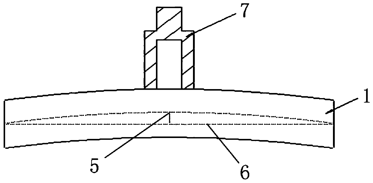
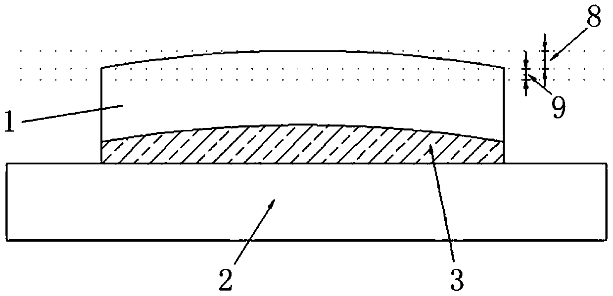
[0030] (1) Patch: such as figure 1 , 2 As shown, the vacuum adsorption device 7 is used to vacuum-adsorb the wafer 1 in an annular manner, and the adsorption area should not be too large, so as to avoid changing the surface shape of the wafer 1 . Apply UV glue 3 evenly on the unadsorbed side of the wafer 1 and lightly press it on the clean and flat ceramic disc 2. The pressure on the wafer must be less than 5kg, so as to avoid pressing the wafer under heavy pressure, which will affect the surface shape of the wafer. Restoration function: irradiate the surface of the wafer 1 with ultraviolet light for 10 seconds until the UV glue 3 is solidified, and then turn off the ultraviolet light.

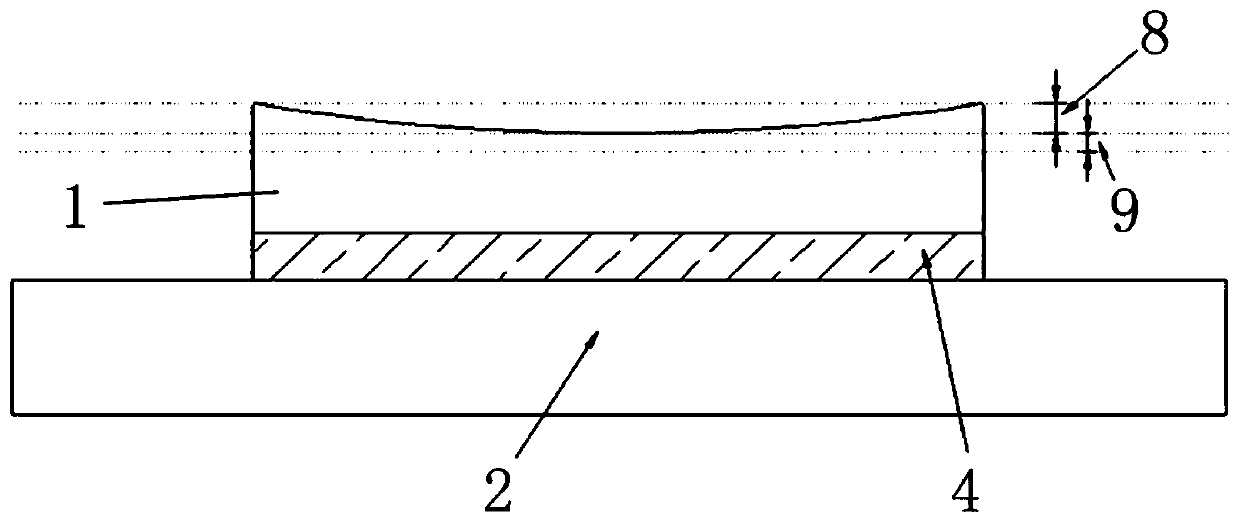
[0031] (2) Single-sided grinding: place the chipped ceramic disc on a single-sided grinding machine, and use the configured boron carbide grinding liquid with a par...


PUM

PropertyMeasurementUnit
particle diameteraaaaaaaaaa

Abstract

The invention discloses a surface type repairing method of a large-sized sapphire substrate wafer. The surface type repairing method of the large-sized sapphire substrate wafer comprises the specificsteps that firstly, one side of the wafer is uniformly coated with UV glue and is lightly pressed onto a ceramic plate, and the surface of the wafer is irradiated with ultraviolet rays until the UV glue is solidified; the wafer on the ceramic plate is subjected to single-side grinding; after the grinding effect is detected, the wafer is removed and cleaned; then the wafer is annealed; and then theside subjected to single-side grinding is uniformly coated a liquid wax, baked and pasted on the ceramic plate; hard polishing is carried out on the other side of the wafer; after the hard polishingeffect is detected, the wax is removed, and cleaning is carried out. The method has good surface type repairing effect on the sapphire substrate wafer, and the grinding amount is small, on the one hand, the warpage of the wafer can be effectively reduced, and on the other hand, the production efficiency and cost can be improved.

Description

technical field [0001] The invention belongs to the field of crystal processing, and in particular relates to a method for repairing the surface shape of a large-size sapphire substrate wafer. Background technique [0002] In the processing of sapphire substrate wafers, the larger the size of the wafer, the greater the warpage of the wafer after slicing. In order to reduce the warpage of the wafer, in the subsequent processing process, the traditional process generally adopts the method of double-sided grinding and single-side hard polishing of the wafer, and repairs the surface of the wafer on both sides to reduce the warpage of the wafer. The purpose of maintaining the flat surface of the wafer. However, the traditional processing technology has the following deficiencies: (1) Due to the good toughness of sapphire after slicing, under the pressure of the double-sided grinding disc, the wafer will be flattened, and both sides of the wafer will be evenly ground. Afterwards...

Claims


Application Information

Patent Timeline
Patent Type & Authority Applications(China)
IPC IPC(8): B24B7/22B24B41/06B24B49/16C30B33/02C30B29/20
CPCB24B7/228B24B41/068B24B49/16C30B29/20C30B33/02
Inventor 陆昌程宋述远蔡金荣
Owner 江苏吉星新材料有限公司
Why Eureka
Try Eureka