A novel tft device structure and manufacturing method thereof

A technology of device structure and manufacturing method, which is applied in the field of microelectronics, can solve the problems affecting the yield rate of the process, and achieve the effects of reducing the probability of light leakage, improving the brightness of the screen, and improving the yield rate of the process

Active Publication Date: 2021-11-23
FUJIAN HUAJIACAI CO LTD
View PDF10 Cites 0 Cited by
  • Summary
  • Abstract
  • Description
  • Claims
  • Application Information

AI Technical Summary

Problems solved by technology

[0002] In the cell (CELL) process, the alignment of polyimide (Polyimide, referred to as PI) because it gives a pretilt angle to the rotation of the liquid crystal makes the rotation direction of the liquid crystal tend to be stable. Therefore, the polyimide alignment film The quality of the coating process is an important link in determining the alignment ability of polyimide, which affects the process yield
The existing thin film transistor (Thin Film Transistor, referred to as TFT) device structure is prone to pits in the TFT device and the "adsorption effect" in the transfer printing (APR) plate during the polyimide coating process, which affects the yield of the process.

Method used


Image

  • A novel tft device structure and manufacturing method thereof
  • A novel tft device structure and manufacturing method thereof

Examples


Embodiment 1

[0048] Please refer to figure 1 , Embodiment 1 of the present invention is:

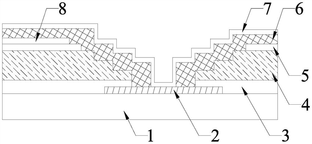
[0049] A new type of TFT device structure, including a substrate 1, on the surface of the substrate 1, a semiconductor layer 2, a first insulating layer 3, a flat layer 4, a second insulating layer 5, a third insulating layer 6 and a transparent conductive layer 7 are sequentially stacked , the vertical section of the flat layer 4 is stepped, and the order of the flat layer 4 is 2-5 layers, preferably 3 layers;

[0050] A via hole is opened on the first insulating layer 3, the via hole is set corresponding to the semiconductor layer 2, and the via hole is symmetrical to the axisymmetric center of the semiconductor layer 2, and the via hole is filled with the The third insulating layer 6 and the transparent conductive layer 7, the third insulating layer 6 is in contact with the semiconductor layer 2, the first insulating layer 3 and the flat layer 2 respectively, and the transparent conductive layer ...

Embodiment 2

[0053] Please refer to figure 2 , the second embodiment of the present invention is:

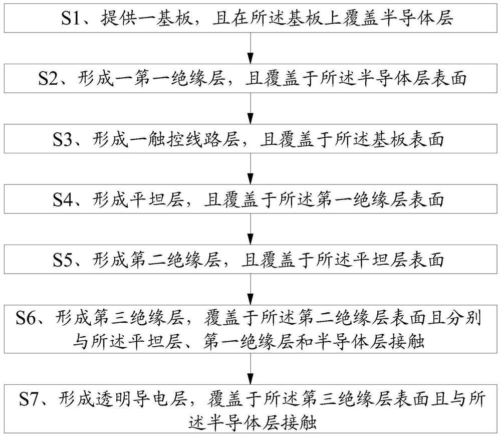
[0054] A method for manufacturing a novel TFT device structure, comprising the following steps:

[0055] S1, providing a substrate 1, and covering the semiconductor layer 2 on the substrate 1;

[0056] S2, forming a first insulating layer 3, and covering the surface of the semiconductor layer 2;

[0057]S3, forming a via hole in the first insulating layer 3;

[0058] S4, forming a flat layer 4 and covering the surface of the first insulating layer 3;

[0059] Step S4 is specifically:

[0060] Place the photomask above the first insulating layer 3, and irradiate the upper surface of the photomask with ultraviolet light to form a stepped flat layer 4, and the flat layer 4 covers the surface of the first insulating layer 3;

[0061] The mask is a half-tone mask, and the number of steps of the flat layer 4 formed by using half-tone masks with different light transmittances is different, an...


PUM


Abstract

The invention relates to the field of microelectronic technology, in particular to a novel TFT device structure and a manufacturing method thereof. By setting a flat layer, the vertical section of the flat layer is stepped, which can reduce the TFT device generated during the polyimide coating process. The "adsorption effect" of the concave hole on the transfer printing (APR) plate enables the transfer printing (APR) plate to have uniform ink and polyimide (PI) alignment film thickness; and can make the liquid crystal rotation direction stable and consistent, which is beneficial It is used to increase the aperture ratio and reduce the probability of light leakage, thereby improving the brightness of the screen. At the same time, the flat layer with a stepped vertical section can reduce the occurrence of panel display anomalies, thereby improving the process yield and helping to increase production capacity.

Description

technical field [0001] The invention relates to the technical field of microelectronics, in particular to a novel TFT device structure and a manufacturing method thereof. Background technique [0002] In the cell (CELL) process, the alignment of polyimide (Polyimide, referred to as PI) is because it gives a pretilt angle to the rotation of the liquid crystal so that the rotation direction of the liquid crystal tends to be stable. Therefore, the polyimide alignment film The quality of the coating process is an important link in determining the alignment ability of polyimide, which affects the process yield. In the existing thin film transistor (Thin Film Transistor, referred to as TFT) device structure, it is easy to cause pits in the TFT device and "adsorption effect" in the transfer printing (APR) plate during the polyimide coating process, which affects the yield of the process. Contents of the invention [0003] The technical problem to be solved by the present inventi...

Claims


Application Information

Patent Timeline
Patent Type & Authority Patents(China)
IPC IPC(8): H01L21/28
CPCH01L21/28
Inventor 官晓蓉曾志远
Owner FUJIAN HUAJIACAI CO LTD
Why Eureka
Try Eureka