Manufacturing method for high reliability VDMOS power device

A technology of power devices and manufacturing methods, applied in semiconductor/solid-state device manufacturing, semiconductor devices, electrical components, etc., can solve problems such as low device reliability, achieve strong operability, strong controllability, and reduce leakage probability Effect

Inactive Publication Date: 2019-11-19
58TH RES INST OF CETC
View PDF0 Cites 0 Cited by
  • Summary
  • Abstract
  • Description
  • Claims
  • Application Information

AI Technical Summary

Problems solved by technology

[0013] The purpose of the present invention is to provide a method for manufacturing a high-reliability VDMOS power device, so as to solve the problem of low reliability of the device produced by the current technology

Method used


Image

  • Manufacturing method for high reliability VDMOS power device
  • Manufacturing method for high reliability VDMOS power device
  • Manufacturing method for high reliability VDMOS power device

Examples


Embodiment 1

[0065]The invention provides a method for manufacturing a high-reliability VDMOS power device. First, an epitaxial silicon layer is grown on a silicon substrate; then a body contact terminal and a source terminal are formed in the epitaxial silicon layer; finally, the contact terminal and the source terminal are formed. The source is connected out.

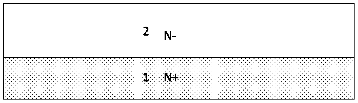
[0066] Specifically, such as Figure 9 As shown, an epitaxial silicon layer 2 is grown on a silicon substrate 1 . The silicon substrate 1 is a silicon substrate with high energy and low resistivity, and its resistivity is 0.002-0.004 Ω·cm, preferably arsenic; the grown epitaxial silicon layer 2 has a resistivity of 3-24 Ohm, and a thickness of 3-24 Ohm. 50 μm.

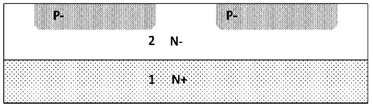
[0067] A shielding layer 9 is deposited on the surface of the epitaxial silicon layer 2, the shielding layer 9 is made of silicon dioxide, nitride or a stack of silicon dioxide and silicon nitride, and its thickness is 200-800nm, such as Figure 10 ;

[0068] Such as ...


PUM

PropertyMeasurementUnit
thicknessaaaaaaaaaa
electrical resistivityaaaaaaaaaa
thicknessaaaaaaaaaa

Abstract

The invention discloses a manufacturing method for a high reliability VDMOS power device, and belongs to the technical field of integrated circuit design. The method includes growing an epitaxial silicon layer on a silicon substrate; depositing a shielding layer on the epitaxial silicon layer; designing a photomask of a P-well pattern, performing corrosion, and removing the redundant shielding layer; manufacturing a P well; depositing a silicon dioxide layer on the surface to perform corrosion to form two side triangular structures; manufacturing a contact end and a source end; and taking outthe contact end and the source end. Through the increasing of the shielding layer and the silicon dioxide layer of a power VDMOS device, the fixing of the effective dimension of a channel can be realized, so that the probability of the occurrence of electric leakage can be reduced; and the method is simple in processing technology and strong in controllability, and has strong maneuverability.

Description

technical field [0001] The invention relates to the technical field of integrated circuit design, in particular to a manufacturing method of a high-reliability VDMOS power device. Background technique [0002] The reliability of power devices is directly related to the safety of the entire power module, especially in the high power state, whether it can be used normally highlights its importance. [0003] In the manufacturing process of VDMOS power devices, a substrate material sheet with relatively thick resistivity is required, and the resistivity and thickness required for silicon epitaxy are performed on the substrate material sheet, and VDMOS power devices are manufactured after completion. The device manufacturing process is usually to generate field oxygen (SiO2), and then perform field oxygen etching to complete the isolation of the active region. Perform P-type impurity implantation on the active region to form a well (Pwell), the channel region of the device and t...

Claims


Application Information

Patent Timeline
Patent Type & Authority Applications(China)
IPC IPC(8): H01L21/336H01L29/06H01L29/78
CPCH01L29/0607H01L29/66712H01L29/7802
Inventor 徐海铭洪根深吴建伟赵文彬徐政吴素贞
Owner 58TH RES INST OF CETC
Why Eureka
Try Eureka