
Edge detection circuit and edge conversion circuit of integrated magnetic isolation chip

An edge detection and magnetic isolation technology, applied in pulse shaping, pulse description, etc., can solve problems affecting data transmission rate, the frequency of square wave signals should not be too high, complex encoding and decoding circuits, etc., to achieve voltage stability and improve stability and reliability, the effect of fast switching speed

Pending Publication Date: 2019-11-29
宜宾市叙芯半导体有限公司
View PDF0 Cites 0 Cited by
  • Summary
  • Abstract
  • Description
  • Claims
  • Application Information

AI Technical Summary

Problems solved by technology

The disadvantage of this scheme is that the decoding circuit needs to identify double pulses and single pulses, and there needs to be a certain distance between double pulses and single pulses, which will affect the data transmission rate (that is, the rising and falling edges of the input square wave signal There must be a certain distance between them, so that the frequency of the square wave signal cannot be too high)
At the same time, the encoding and decoding circuits are relatively complicated

Method used


Image

  • Edge detection circuit and edge conversion circuit of integrated magnetic isolation chip
  • Edge detection circuit and edge conversion circuit of integrated magnetic isolation chip
  • Edge detection circuit and edge conversion circuit of integrated magnetic isolation chip

Examples


Embodiment Construction

[0036] Existing edge detection circuits use the delay effect of digital logic gates to generate short pulses, such as Figure 4 and Figure 5 shown, where Figure 4 Used to detect the rising edge of the input square wave, Figure 5 Used to detect the falling edge of the input square wave. The input square wave signal reaches the AND gate or the NOR gate through two channels, one channel arrives directly, and the other channel passes through an odd number of inverters to delay and invert the input square wave, and finally obtain an AND rising signal at the output terminal of the AND gate. A short pulse corresponding to the edge, and a short pulse corresponding to the falling edge is obtained at the output of the NOR gate. The duration of the pulse depends on the delay time of the delay circuit. The role of the capacitor is to increase the delay time of the delay circuit. There is an obvious disadvantage of using an inverter for time delay, that is, the time delay of the in...


PUM


Abstract

The invention discloses an edge detection circuit and an edge conversion circuit of an integrated magnetic isolation chip, and relates to the integrated circuit technology. The invention comprises: afirst PMOS transistor, the source of which is connected with a reference high level, the drain of which is connected with the source of a second PMOS transistor, and the gate of which is connected with a signal input end and a first output point; the drain electrode of the second PMOS tube is connected with the second reference point, and the grid electrode of the second PMOS tube is connected with the grid electrode and the drain electrode of the third PMOS tube; the source electrode of the third PMOS transistor is connected with a reference high level, and the drain electrode of the third PMOS transistor is grounded through a first current source; the source electrode of the fourth NMOS transistor is grounded, the grid electrode and the drain electrode of the fourth NMOS transistor are connected with the grid electrode of the fifth NMOS transistor, and the drain electrode of the fourth NMOS transistor is further connected with the output end of the second current source; the source electrode of the fifth NMOS transistor is connected with the drain electrode of the sixth NMOS transistor, the drain electrode of the fifth NMOS transistor is connected with the second output point, and the drain electrode of the fifth NMOS transistor is grounded through a capacitor; and the source electrode of the sixth NMOS transistor is grounded, and the grid electrode of the sixth NMOS transistor is connected with the signal input end. The invention has the advantages that the voltage is relatively stable, the problem of charging and discharging of a drain parasitic capacitor is avoided, the switching speed is high, and the problem of charge shunting is avoided. Meanwhile, the problem of digital control signal charge injection is solved.

Description

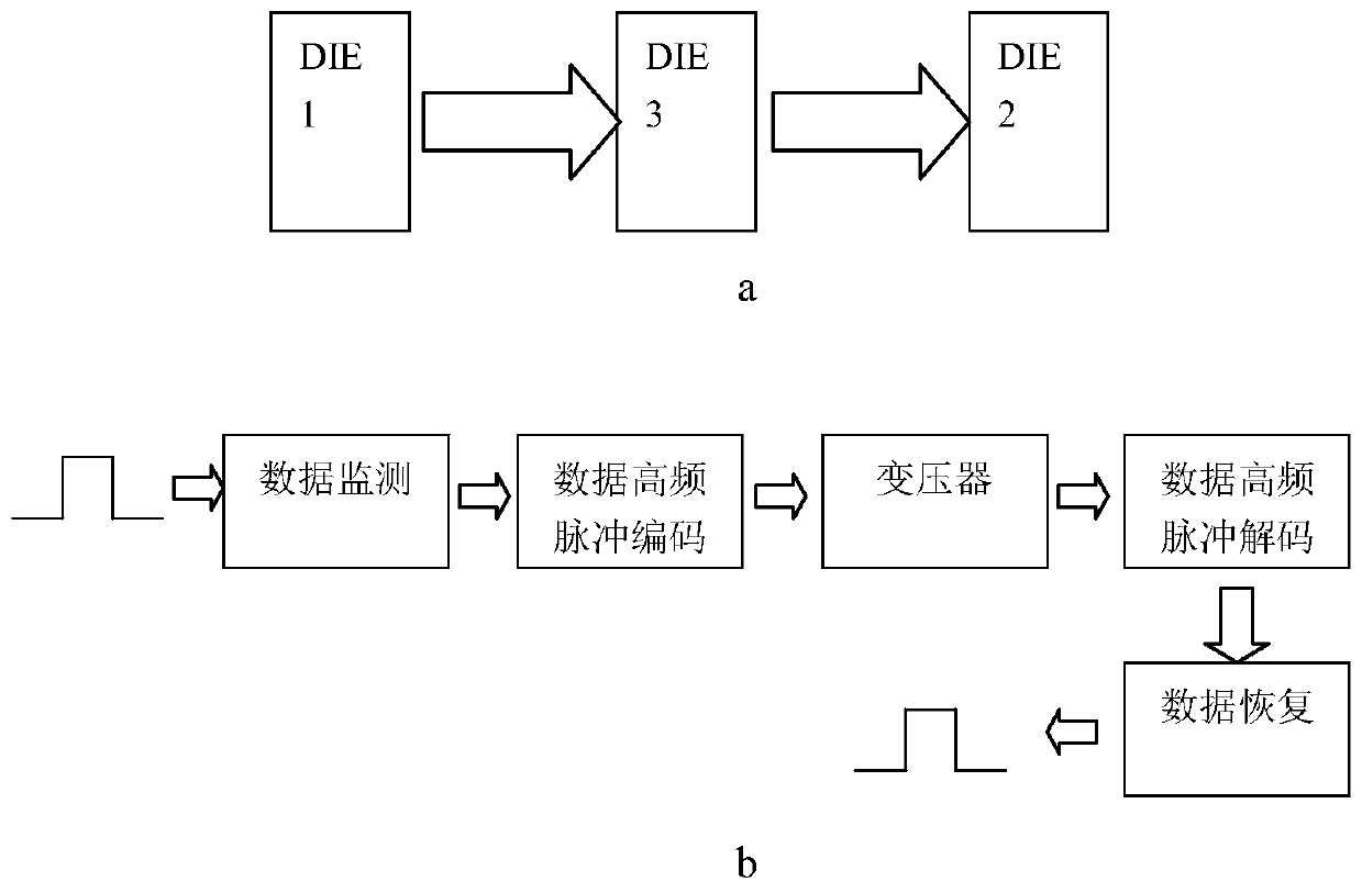
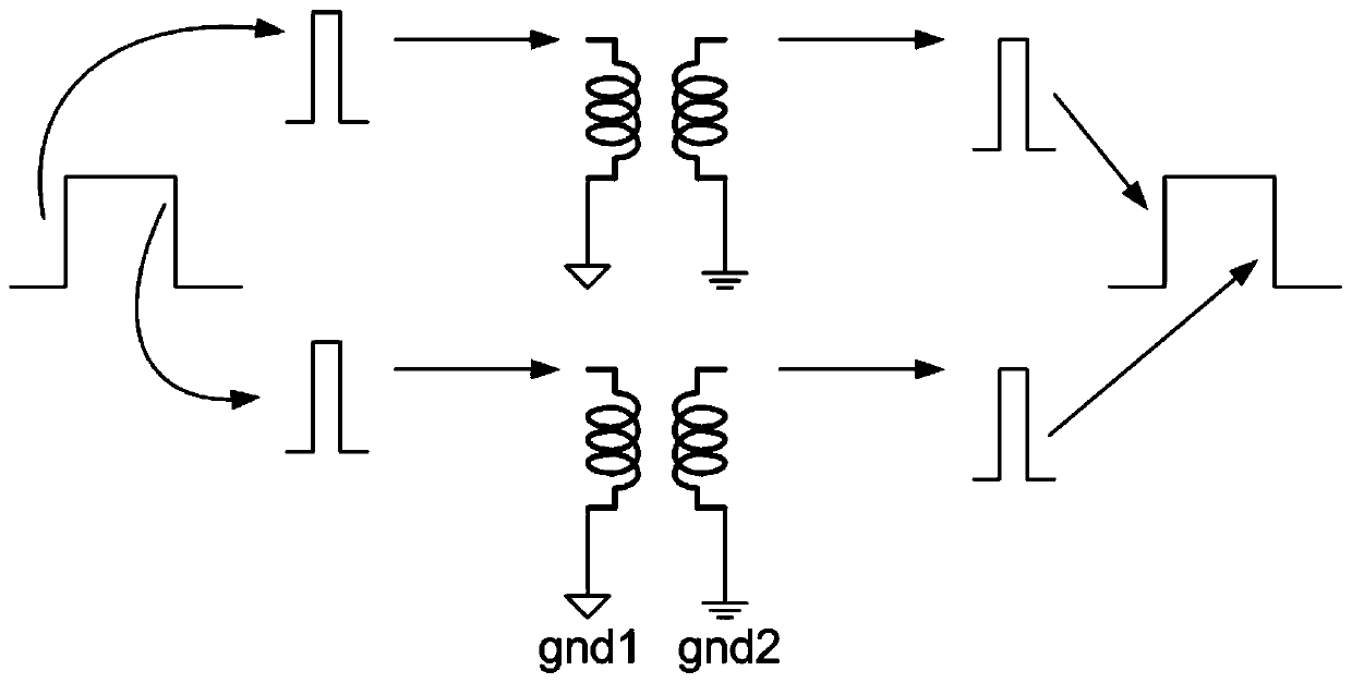
technical field [0001] The present invention relates to integrated circuit technology. Background technique [0002] The function of the isolator is to isolate the circuit modules with independent functions in the circuit system in medical, communication, industrial bus control and other occasions, avoiding the mutual influence between each functional module, and protecting sensitive circuits from dangerous voltage and current damage. exist figure 2 , image 3 and Figure 4 Two grounds are shown in , gnd1 and gnd2, which can be at different potentials. [0003] The circuit isolation device that has been used in large quantities for a long time is an optocoupler device, but the short life of the optocoupler device, low data transmission rate, unstable performance, and excessive volume have obvious disadvantages. [0004] A new isolation method that has emerged in the past decade is to use an on-chip integrated transformer as an isolation device for isolation, that is, ma...

Claims


Application Information

Patent Timeline
Patent Type & Authority Applications(China)
IPC IPC(8): H03K5/125H03K5/06
CPCH03K5/125H03K5/06
Inventor 王佐袁思彤文守甫王建斌罗和平程瑜李威
Owner 宜宾市叙芯半导体有限公司
Learn More