Electrically excited photonic crystal surface emitting type laser element

A photonic crystal and electric excitation technology, which is applied in the direction of electrical components, laser components, lasers, etc., can solve complex technical problems

Active Publication Date: 2019-12-03
PHOSERTEK CORP
View PDF8 Cites 6 Cited by
  • Summary
  • Abstract
  • Description
  • Claims
  • Application Information

AI Technical Summary

Problems solved by technology

[0005] However, due to the fact that the current research on the production of electro-excited photonic crystal lasers is

Method used


Image

  • Electrically excited photonic crystal surface emitting type laser element
  • Electrically excited photonic crystal surface emitting type laser element
  • Electrically excited photonic crystal surface emitting type laser element

Examples


Embodiment Construction

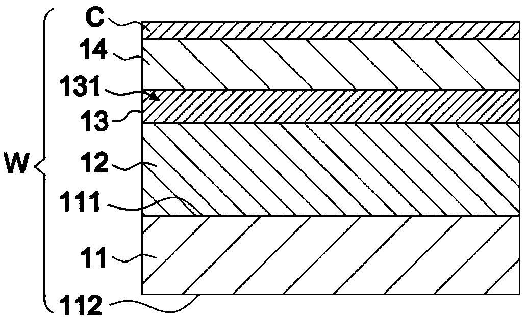
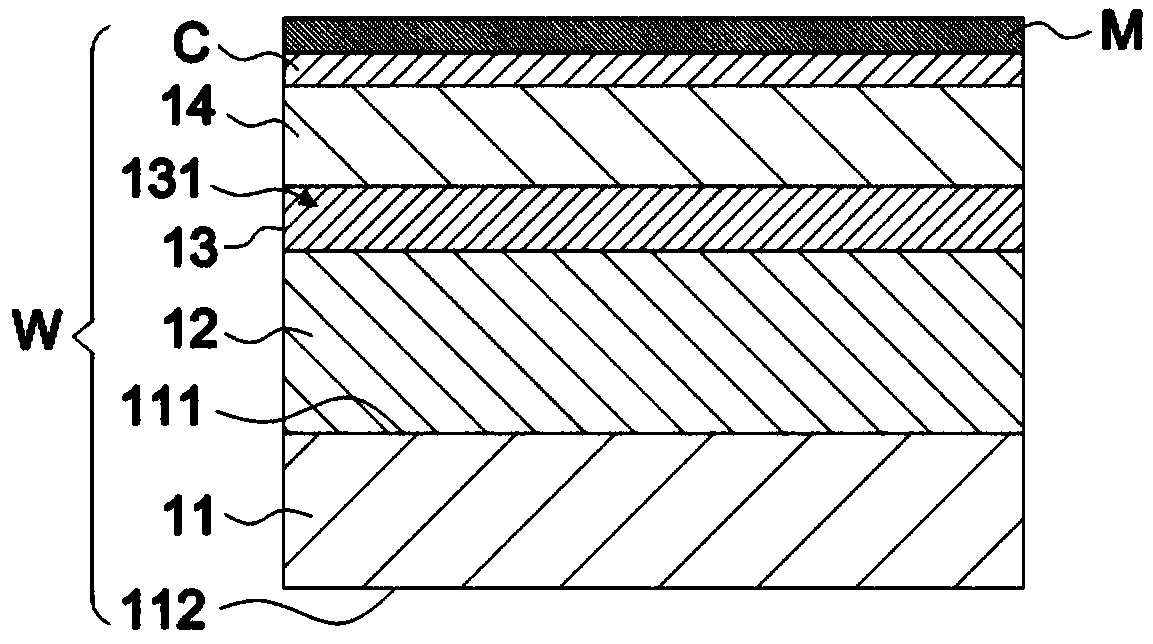
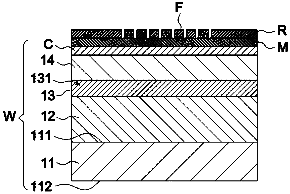
[0083] First, see Figure 1A ~ Figure 1L As shown, a preferred embodiment of an Electrically Pumped Photonic-Crystal Surface-Emitting Laser (Electrically Pumped Photonic-Crystal Surface-Emitting Lasers) component 10A of the present invention includes: a substrate 11 having a first surface 111 and the second surface 112 on the opposite side. In this embodiment, the material of the substrate 11 includes any one of gallium nitride (GaN), gallium arsenide (GaAs), and indium phosphide (InP). Not limited to this.

[0084] A cladding layer (Cladding layer) 12 is located on the first surface 111 of the substrate 11. In this embodiment, the material of the cladding layer 12 includes aluminum gallium arsenide (AlGaAs), gallium arsenide ( GaAs), aluminum gallium nitride (AlGaN), aluminum gallium indium arsenide (AlGaInAs), aluminum gallium indium phosphide (AlGaInP), but not limited thereto.

[0085] An active layer 13 is located on the lower cladding layer 12 and has a quantum structu...


PUM

PropertyMeasurementUnit
Thicknessaaaaaaaaaa

Abstract

An electrically excited photonic crystal surface emitting type laser element comprises: a current limiting structure which is located on a photonic crystal structure and an active layer and is provided with an aperture; a transparent conducting layer positioned on the current limiting structure and covering the photonic crystal structure; and positive electrode metal positioned on the transparentconductive layer and provided with a metal hole. According to the invention, the photonic crystal is manufactured by directly etching from the uppermost part of the epitaxial structure to the inside;a complex technology of wafer fusion or epitaxial growth is not needed, laser light can penetrate the photonic crystal structure and has conductivity, the quantum structure is electrically excited, light can be emitted from the front face of the epitaxial structure through the photonic crystal structure, and the photonic crystal structure has the excellent characteristics of being small in far-field divergence angle and the like.

Description

technical field [0001] The present invention relates to an electro-excited photonic crystal surface-emitting laser element. The positive electrode metal, transparent conductive layer, and current confinement structure cooperate with each other to electrically excite the quantum structure, and then use the photonic crystal structure to make the light energy flow from The front side of the epitaxial structure emits light. Background technique [0002] Photonic crystal (Photonic crystal, PC) is an artificial crystal, or called metamaterials (Metamaterials), the refractive index of this crystal has a periodic distribution in space, and its characteristics are similar to solid crystals. The periodic potential and boundary conditions are introduced into the Schrodinger equation, and the dispersion relation (or band structure) of the solid crystal can be obtained by solving the characteristic problem. In the same way, the energy band structure of photonic crystals can be obtained ...

Claims


Application Information

Patent Timeline
IPC IPC(8): H01S5/18H01S5/323
CPCH01S5/18H01S5/323
Inventor 林国瑞徐铭扬陈俞谌
Owner PHOSERTEK CORP
Why Eureka
Try Eureka