Manufacturing method of circuit board taking boss as bonding pad

A manufacturing method and pad technology, which are applied in printed circuit manufacturing, printed circuits, printed circuits, etc., can solve the problems of poor solder mask thickness uniformity in the screen printing process, low rigidity of photosensitive ink materials, and low glass temperature transition point. Achieve the effect of being conducive to precision packaging, high glass temperature transition point, and small deformation

Active Publication Date: 2019-12-03
NINGBO HUAYUAN ELECTRONICS TECH
View PDF13 Cites 9 Cited by
  • Summary
  • Abstract
  • Description
  • Claims
  • Application Information

AI Technical Summary

Problems solved by technology

[0004] 2. The photosensitive ink for solder resist needs to use screen printing, the solid waste of the ink needs to be treated, and the screen needs to be cleaned and disposed of, which is not environmentally friendly;
[0005] 3. The uniformity of the solder mask thickness of the screen printing process is poor, generally within ±10um, and the surface is uneven, and there will be unevenness;
[0006] 4. The copper surface after the window is opened is prone to residual ink during the ink development process, which leads to the inability to plate the surface of the pad in the subsequent surface treatment process;
[0007] 5. Side erosion is unavoidable on the edge of the window, and the thicker the ink, the greater the side erosion;
[0008] 6. The rigidity of the photosensitive ink material is low, and the glass temperature transition point is low, resulting in a high degree of thermal expansion of the product in the high-temperature process, which is not conducive to the high-precision packaging process;
[0009] 7. Due to the tolerance of solder mask exposure alignment, it is not conducive to the production of small-area and high-density pads

Method used


Image

  • Manufacturing method of circuit board taking boss as bonding pad
  • Manufacturing method of circuit board taking boss as bonding pad

Examples


Embodiment Construction

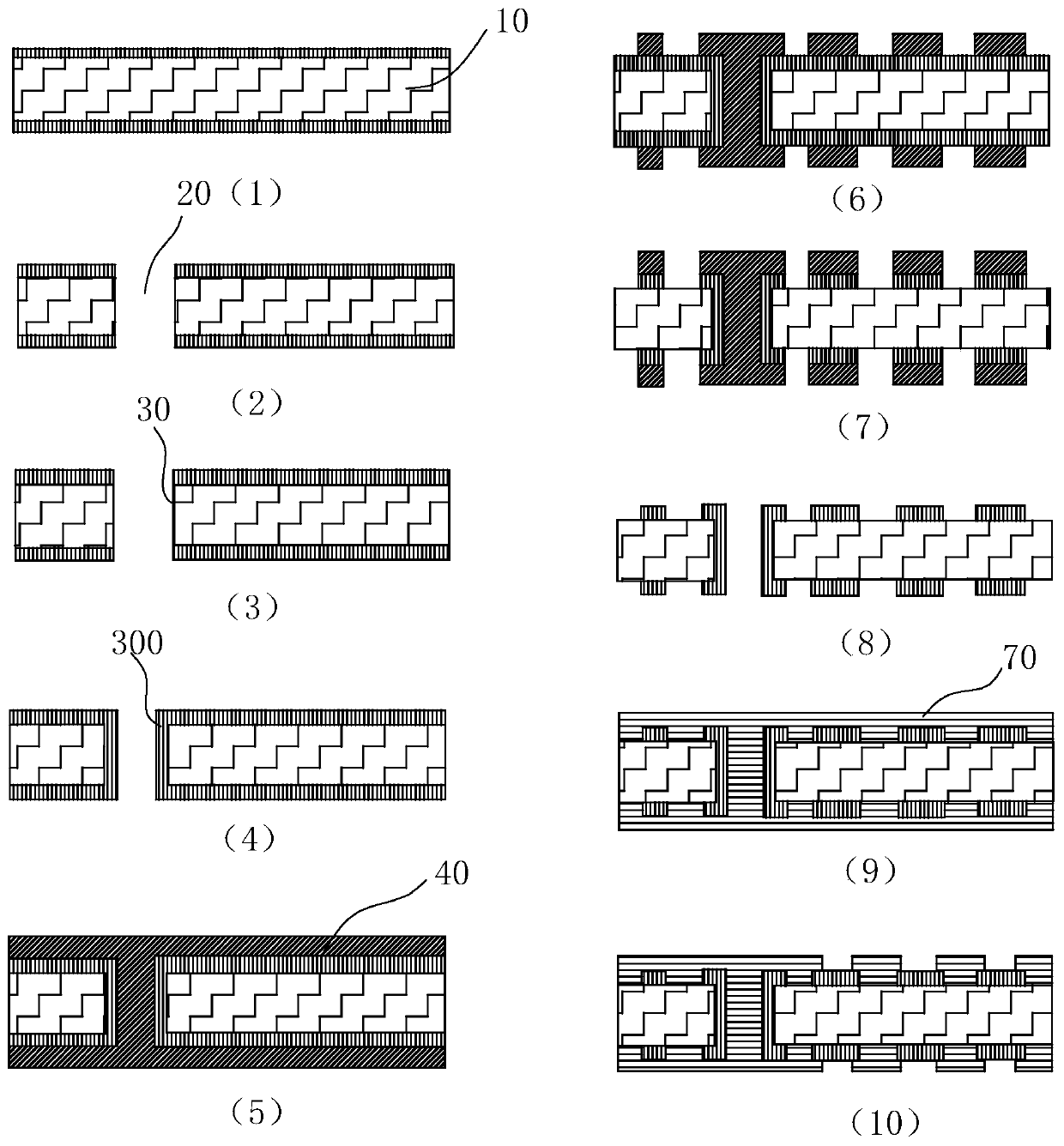
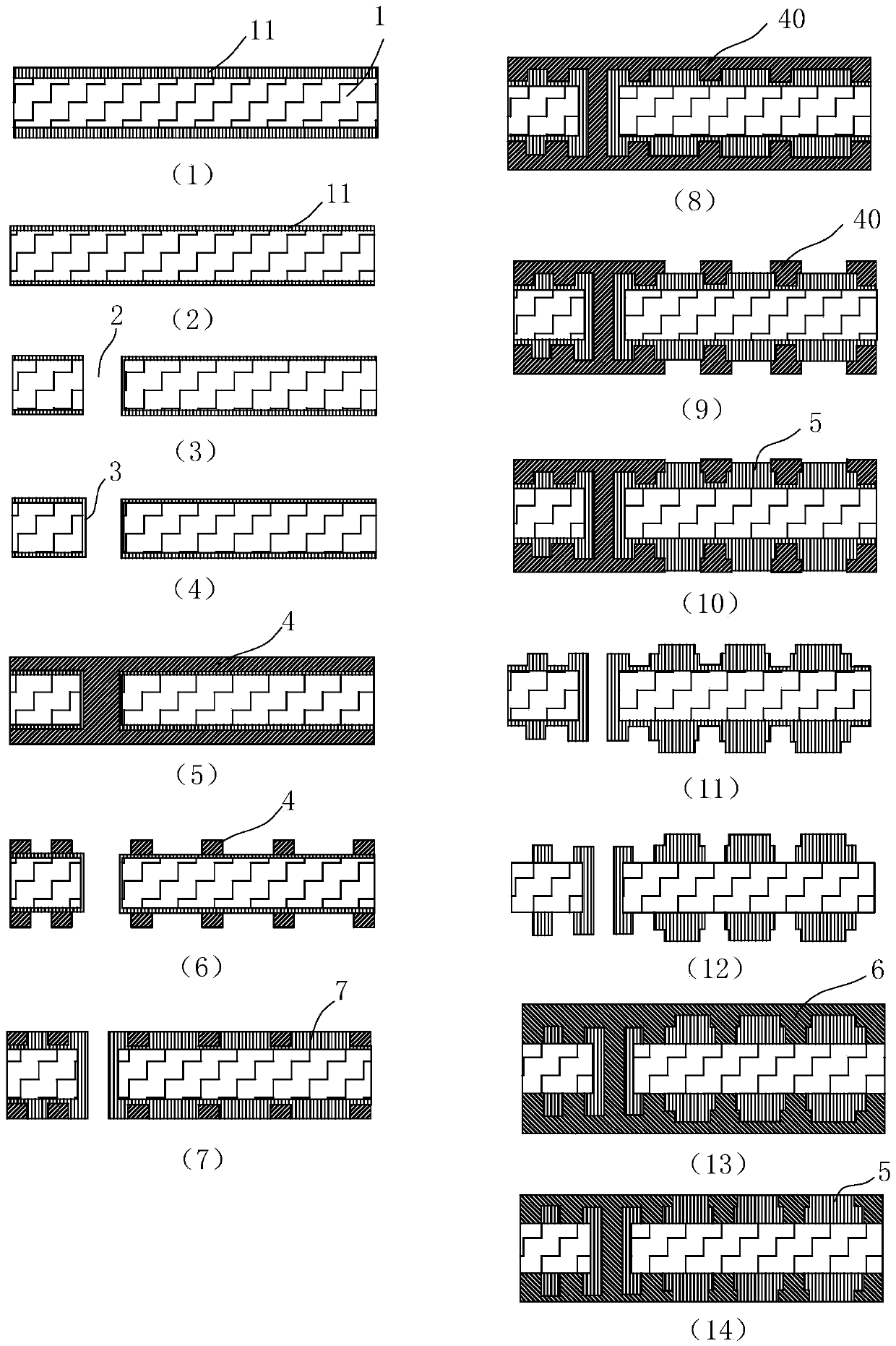
[0036] The present invention will be further described in detail below in conjunction with the accompanying drawings and embodiments.

[0037] Such as figure 2 As shown, a method for making a circuit board with a boss as a pad comprises the following steps:

[0038] 1) Cutting: blanking of base material 1, base material 1 can be single-layer board, multi-layer board, soft-hard board or hard board, such as figure 2 (1);

[0039] 2) Copper reduction: thinning the copper layer 11 on the surface of the substrate 1, after the copper reduction, the thickness of the remaining copper layer 11 is 1-2 μm, such as figure 2 (2);

[0040] 3) Drilling: drill hole 3 at the position where interlayer conduction is required, such as figure 2 (3);

[0041] 4) Immersion copper: deposit a layer of conductive copper layer 3 on the insulating layer of the hole wall, with a thickness of 0.3-1.0 μm, such as figure 2 (4);

[0042] 5) Lamination: press a photosensitive dry film 4, and press ...


PUM


Abstract

The invention discloses a manufacturing method of a circuit board taking a boss as a bonding pad. The manufacturing method comprises the following steps of cutting and reducing copper; drilling a hole; carrying out copper deposition; pressing a film; exposing and developing; carrying out circuit electroplating; pressing the film; exposing and developing; electroplating the bonding pad; demouldingand removing copper; laminating an insulating layer; and grinding: grinding a surface of the insulating layer till that the bonding pad is exposed, and forming a top layer / bottom layer bonding pad through windowing. A thermosetting insulating material is adopted, cost is low, silk-screen is not needed, green and environmental protection performance is achieved, and simultaneously, a manufacturingprocess is simple, operation is easy, the bonding pad is directly manufactured through grinding, the bonding pad with a small area and a large density can be conveniently manufactured, a manufacturedcircuit board is smooth in surface, precise packaging is facilitated, circuit attachment is firm, and quality is good.

Description

technical field [0001] The invention belongs to the technical field of circuit board production, and relates to a circuit board, in particular to a method for producing a circuit board with bosses as pads. Background technique [0002] With the continuous advancement of technology, the functional requirements of electronic products are getting higher and higher. During the preparation process of the circuit board, it is often necessary to make bosses as pads. The existing manufacturing methods are as follows: figure 1 As shown, the process is: cutting (substrate 10 blanking) → drilling 20 → copper sinking (depositing a layer of conductive copper layer 30 on the hole wall insulation layer) → copper plating (thickening the hole copper thickness and surface Copper thickness 300)→lamination (pressure-sensitive dry film 40)→exposure, development (remove the dry film 40 in the non-circuit area)→etching (remove the copper layer in the non-circuit area)→remove the film (remove the ...

Claims


Application Information

Patent Timeline
Patent Type & Authority Applications(China)
IPC IPC(8): H05K3/40H05K3/06H05K1/11
CPCH05K3/4007H05K3/06H05K1/111H05K2201/09845
Inventor 张成立徐光龙王强李东海茆昊奇黄礼树
Owner NINGBO HUAYUAN ELECTRONICS TECH
Why Eureka
Try Eureka