MEMS wafer-level vacuum packaging method

A vacuum packaging, wafer-level technology, applied in decorative arts, measuring devices, microstructure devices, etc., can solve the problems of low vacuum degree of vacuum packaging, high gas leakage rate, and difficulty in maintaining vacuum degree for a long time, so as to improve the degree of vacuum , the effect of solving the problem

Inactive Publication Date: 2019-12-13
EAST CHINA INST OF OPTOELECTRONICS INTEGRATEDDEVICE
View PDF12 Cites 3 Cited by
  • Summary
  • Abstract
  • Description
  • Claims
  • Application Information

AI Technical Summary

Problems solved by technology

[0006] The purpose of the present invention is to provide a MEMS wafer-level vacuum packaging method, which can solve the problems of low vacuum degree, high gas leakage rate and difficulty in maintaining vacuum degree for a long time in existing vacuum packaging.

Method used


Image

  • MEMS wafer-level vacuum packaging method
  • MEMS wafer-level vacuum packaging method
  • MEMS wafer-level vacuum packaging method

Examples


Embodiment Construction

[0048] The invention provides a MEMS wafer-level vacuum packaging method, comprising the following steps:

[0049] S1, preparing the substrate layer,

[0050] Follow the sub-steps below:

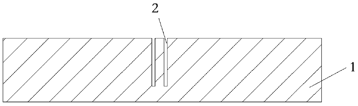
[0051] S11, such as figure 1 As shown, a double-polished silicon wafer with a thickness of 300-400 μm is used as the substrate layer silicon wafer 1, and an annular groove 2 is etched in the center of the top surface of the substrate layer silicon wafer 1 by photolithography; the depth of the annular groove 2 is 200-300 μm;

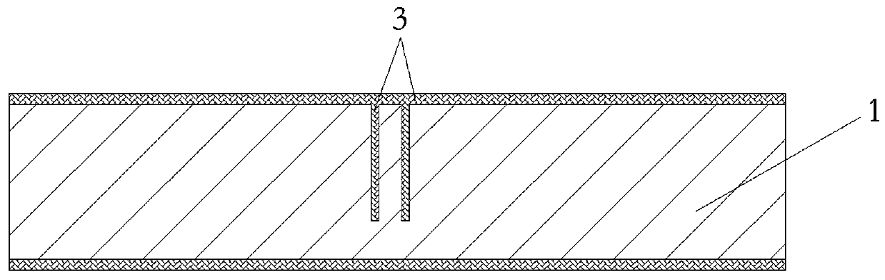
[0052] S12. Combination figure 2 As shown, an insulating layer with a thickness of 0.5 to 1 μm is grown on the side wall of the annular groove 2 by an oxidation process, and then polysilicon 3 is deposited on the surface of the substrate layer silicon wafer 1 by an LPCVD process to fill the annular groove 2;

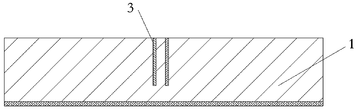
[0053] S13. Combination image 3 As shown, the front surface of the silicon wafer 1 of the substrate layer is polished by a CMP process to expose the surface...


PUM


Abstract

The invention discloses an MEMS wafer-level vacuum packaging method, which comprises the following steps: S1, manufacturing a substrate layer: manufacturing an annular groove filled with an insulatingmedium on a double-polished silicon wafer to form a silicon vertical lead, and etching a deep cavity to serve as an activity space of an MEMS movable structure; S2, manufacturing a structural layer;S3, manufacturing a cap layer: manufacturing a vacuum chamber and a vacuum buffer chamber on the front surface of the double-polished silicon wafer, then manufacturing a Ti / Au gold-silicon bonding ring, and finally preparing a getter layer in the vacuum chamber and the vacuum buffer chamber; and S4, vacuum packaging: performing a gold-silicon bonding process on the prepared cap and the structure layer to complete MEMS wafer-level vacuum packaging, and finally preparing gold welding spots for lead bonding; the vacuum degree of the MEMS device is improved through the vacuum chamber and the vacuum buffer chamber, and excessive gas is absorbed by the getter, so that the vacuum degree can be kept for a long time.

Description

technical field [0001] The invention relates to the technical field of MEMS vacuum packaging, in particular to a MEMS wafer-level vacuum packaging method. Background technique [0002] Micro-Electro Mechanical Systems (MEMS) is a high-tech electronic mechanical product developed on the basis of microelectronics technology, which combines photolithography, etching, film formation, silicon micromachining and other technologies. It has become a recent research hotspot due to its advantages of small size, low power consumption, and good integration. [0003] For most MEMS products, vacuum packaging is the key to determine its final volume, protect the internal structure, and provide a stable working environment, and is an important factor affecting the performance of the product. MEMS vacuum packaging is divided into two forms: device-level packaging and wafer-level packaging. Wafer-level packaging is a packaging method in which MEMS structure wafers are first vacuum-packaged ...

Claims


Application Information

Patent Timeline
IPC IPC(8): B81C1/00B81B7/00
CPCB81C1/00261B81C1/00269B81C1/00277B81C1/00285B81C1/00301B81B7/0035B81B7/0038B81B7/007
Inventor 王帆刘磊张帅喻磊郭立建张伟房立峰
Owner EAST CHINA INST OF OPTOELECTRONICS INTEGRATEDDEVICE
Why Eureka
Try Eureka