Semiconductor structure and formation method thereof

A technology of semiconductor and channel structure, which is applied in the direction of semiconductor devices, semiconductor/solid-state device manufacturing, electrical components, etc., can solve the problems of device performance to be improved, and achieve the effect of improving device performance, improving performance, and reducing space size

Active Publication Date: 2019-12-17
SEMICON MFG INT (SHANGHAI) CORP +1
View PDF5 Cites 3 Cited by
  • Summary
  • Abstract
  • Description
  • Claims
  • Application Information

AI Technical Summary

Problems solved by technology

[0005] However, after introducing the barrier layer

Method used


Image

  • Semiconductor structure and formation method thereof
  • Semiconductor structure and formation method thereof
  • Semiconductor structure and formation method thereof

Examples


Embodiment Construction

[0016] It can be seen from the background art that after the barrier layer is introduced between the gate electrode and the source-drain doped layer, the performance of the device still needs to be improved. Combining with a semiconductor structure, the reason why the performance of the device still needs to be improved is analyzed.

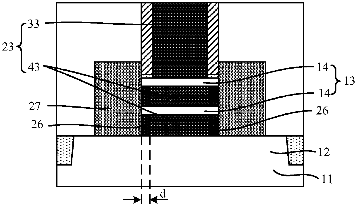
[0017] refer to figure 1 , shows a schematic structural view of a semiconductor structure.

[0018] The semiconductor structure includes: a substrate 11; a fin 12 protruding from the surface of the substrate 11; a channel structure layer 13 located on the fin 12 and spaced apart from the fin 12, the trench The channel structure layer 13 includes a plurality of channel layers 14 arranged at intervals; a metal gate structure 23 across the channel structure layer 13, the metal gate structure 23 is located on the fin portion 12 and surrounds the channel layer 14, and along the extending direction of the fin 12, the metal gate structure 23 exposes t...


PUM

PropertyMeasurementUnit
Thicknessaaaaaaaaaa
Thicknessaaaaaaaaaa

Abstract

The invention discloses a semiconductor structure and a formation method thereof. The method comprises the steps of providing a substrate, a fin portion and channel laminations located on the fin portion, wherein each channel lamination comprises sacrificial layers and channel layers, if the number of the channel laminations is two, the sacrificial layer close to the top of the channel laminationis a first sacrificial layer, the remaining sacrificial layer is a second sacrificial layer, and if the number of the channel laminations is greater than or equal to three, at least one sacrificial layer close to the top of the channel lamination is a first sacrificial layer, and the remaining sacrificial layers are second sacrificial layers; forming a pseudo gate structure; etching the channel lamination layers on two sides of the pseudo gate structure to form grooves; etching part of the first sacrificial layer exposed out of the groove to form a first trench; forming a first barrier layer in the first trench; etching part of the second sacrificial layer exposed out of the groove to form a second trench, wherein the depth of the second trench is greater than that of the first trench; forming a second barrier layer in the second trench; forming a source-drain doping layer in the groove; and forming a metal gate structure at the positions of the pseudo gate structure, the remaining first sacrificial layer and the remaining second sacrificial layer. The forming quality of the metal gate structure is improved according to the invention.

Description

technical field [0001] The invention relates to the field of semiconductor manufacturing, in particular to a semiconductor structure and a forming method thereof. Background technique [0002] In semiconductor manufacturing, with the development trend of VLSI, the feature size of integrated circuits continues to decrease. In order to better meet the requirements of scaling down the device size, the semiconductor process has gradually begun to transition from planar transistors to three-dimensional transistors with higher efficiency, such as forming a gate-all-around gate with fins (Gate-all-around, GAA) transistor. In a fully surrounded gate transistor, the gate surrounds the area where the channel is located. Compared with a planar transistor, the gate of a fully surrounded gate transistor has a stronger ability to control the channel and can better suppress the short channel effect. . [0003] When the size of semiconductor devices is reduced to a certain extent, how to...

Claims


Application Information

Patent Timeline
IPC IPC(8): H01L29/78H01L21/336
CPCH01L29/785H01L29/66795
Inventor 周飞
Owner SEMICON MFG INT (SHANGHAI) CORP
Why Eureka
Try Eureka