A kind of oled structure and manufacturing method thereof

A hole injection layer and film layer technology, applied in the field of OLED, can solve problems such as affecting current efficiency, device short circuit, poor film uniformity, etc., to achieve the effect of improving yield level, improving uniformity, and reducing step difference

Active Publication Date:
View PDF1 Cites 0 Cited by
  • Summary
  • Abstract
  • Description
  • Claims
  • Application Information

AI Technical Summary

Problems solved by technology

[0002] In the existing organic electroluminescent diode (OLED) preparation process, due to the large step difference and slope of the organic film layer at the edge of the light-emitting area (Edge), this makes the uniformity of the cathode (Cathode) film layer at the Edge part poor and there are A certain stress and a large step difference will also lead to poor packaging effect, which will eventually affect the current efficiency, or cause the device to short circuit or enter into water / oxygen and be scrapped, affecting the yield level of the product

Method used


Image

  • A kind of oled structure and manufacturing method thereof
  • A kind of oled structure and manufacturing method thereof

Examples


Embodiment Construction

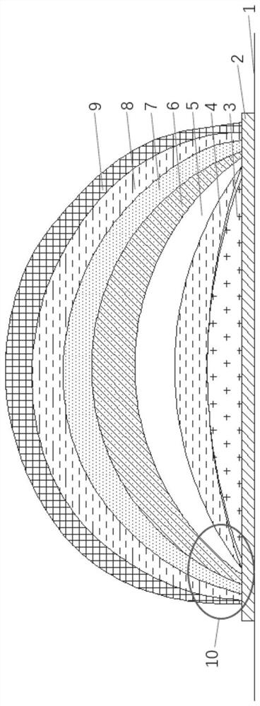
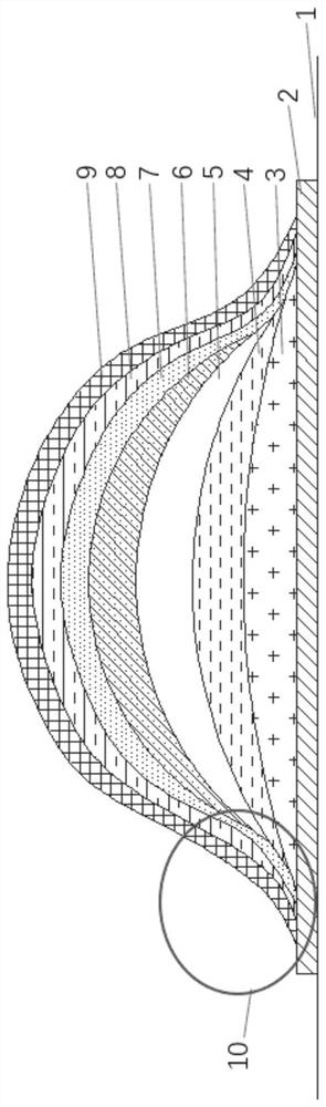
[0026] Such as figure 2 As shown, the OLED structure of the present invention includes a substrate 1, a layer of anode 2 is deposited on the substrate 1, and a hole injection layer 3, a hole transport layer 4, a light-emitting layer 5, and an electron transport layer 6 are sequentially deposited on the anode 2 , the structure of the hole injection layer 3, the hole transport layer 4, the light emitting layer 5, and the electron transport layer 6 is distributed in a trapezoid, and the area of ​​each layer gradually decreases from bottom to top; the electron injection layer 7 and the electron transport layer are deposited on the electron transport layer 6. Metal cathode 8, the area of ​​electron injection layer 7 is larger than that of hole injection layer 3, and the area of ​​metal cathode 8 is larger than that of electron injection layer 7; finally aluminum oxide and silicon nitride encapsulation layer 9 are sequentially deposited on the metal cathode.

[0027] The manufactur...


PUM

PropertyMeasurementUnit
thicknessaaaaaaaaaa
thicknessaaaaaaaaaa

Abstract

The present invention relates to the technical field of OLEDs, in particular to an OLED structure comprising a base, on which a layer of anode is deposited, on which a hole injection layer, a hole transport layer, a light-emitting layer, and an electron transport layer are sequentially deposited. The structure of the hole injection layer, the hole transport layer, the light-emitting layer, and the electron transport layer is distributed in a trapezoid, and the area of ​​each layer decreases gradually from bottom to top; an electron injection layer and a metal cathode are deposited on the electron transport layer, and the area of ​​the electron injection layer is larger than the hole injection layer, and the area of ​​the metal cathode is larger than that of the electron injection layer; finally, an aluminum oxide packaging layer and a silicon nitride packaging layer are sequentially deposited on the metal cathode. After adopting the above-mentioned structure and method, the present invention optimizes the film structure of the OLED device, reduces the step difference and slope of the organic film layer in the edge part of the light-emitting area, can significantly improve the uniformity of the metal cathode film layer in the edge part, and reduce the stress between the film layers , Improve product yield level.

Description

technical field [0001] The invention relates to the technical field of OLEDs, in particular to an OLED structure and a manufacturing method thereof. Background technique [0002] In the existing organic electroluminescent diode (OLED) preparation process, due to the large step difference and slope of the organic film layer at the edge of the light-emitting area (Edge), this makes the uniformity of the cathode (Cathode) film layer at the Edge part poor and there are A certain stress and a large step difference will also lead to poor packaging effect, which will eventually affect the current efficiency, or cause the device to short circuit or enter water / oxygen and be scrapped, affecting the yield level of the product. [0003] Chinese invention patent CN 107068905 A discloses an OLED packaging structure, including a substrate on which an OLED structure to be packaged is arranged; an inorganic cover layer is arranged on the substrate and the OLED structure so that the edge por...

Claims


Application Information

Patent Timeline
Patent Type & Authority Patents(China)
IPC IPC(8): H01L51/50H01L51/52H01L51/56
CPCH10K50/15H10K50/16H10K50/17H10K50/171H10K50/11H10K50/82H10K50/844H10K71/00
Inventor 王绍华褚天舒汪烨辰
Why Eureka
Try Eureka